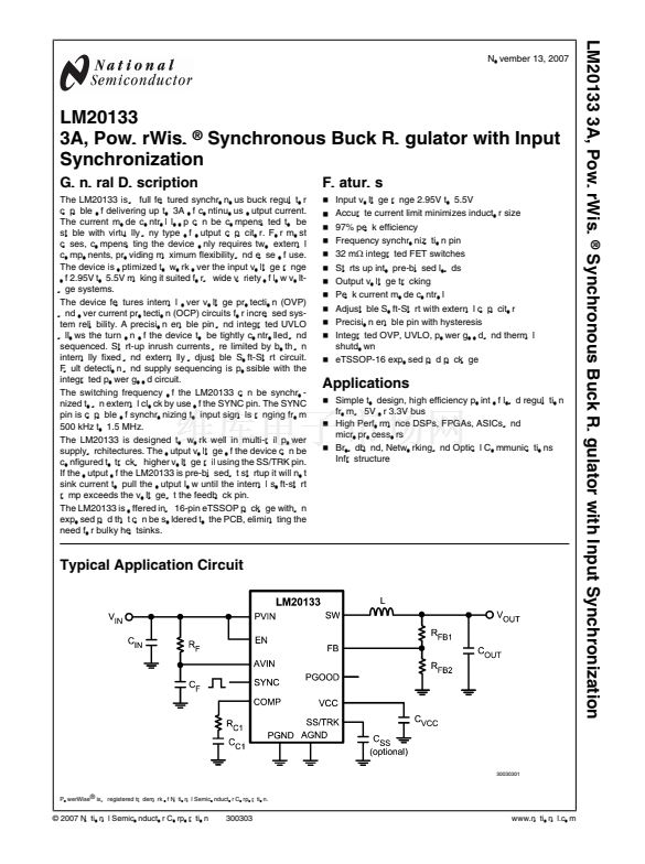
LM20133
Design Guide
This section walks the designer through the steps necessary
to select the external components to build a fully functional
power supply. As with any DC-DC converter numerous trade-
offs are possible to optimize the design for efficiency, size, or
performance. These will be taken into account and highlight-
ed throughout this discussion. To facilitate component selec-
tion discussions the circuit shown in
Figure 2
below may be
used as a reference. Unless otherwise indicated all formulas
assume units of amps (A) for current, farads (F) for capaci-
tance, henries (H) for inductance and volts (V) for voltages.
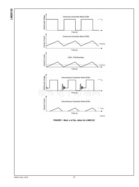
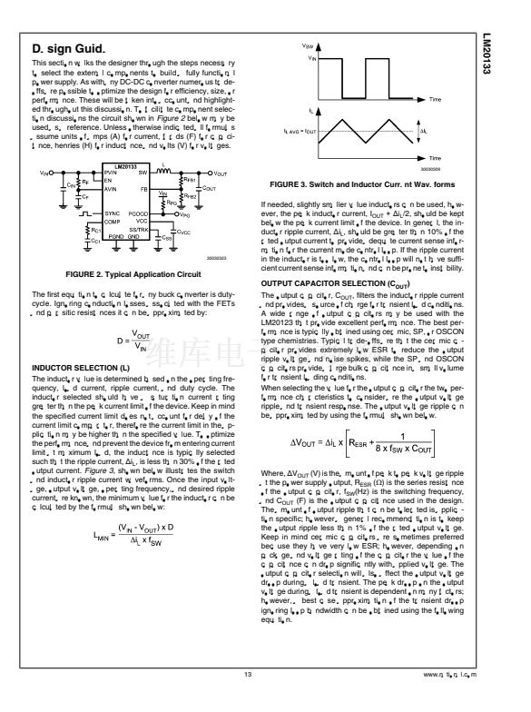
30030309
FIGURE 3. Switch and Inductor Current Waveforms
If needed, slightly smaller value inductors can be used, how-
ever, the peak inductor current, I
OUT
+ 螖i
L
/2, should be kept
below the peak current limit of the device. In general, the in-
ductor ripple current,
螖i
L
, should be greater than 10% of the
rated output current to provide adequate current sense infor-
mation for the current mode control loop. If the ripple current
in the inductor is too low, the control loop will not have suffi-
cient current sense information and can be prone to instability.
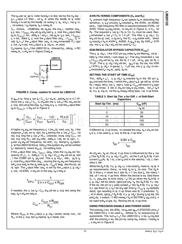
OUTPUT CAPACITOR SELECTION (C
OUT
)
The output capacitor, C
OUT
, filters the inductor ripple current
and provides a source of charge for transient load conditions.
A wide range of output capacitors may be used with the
LM20123 that provide excellent performance. The best per-
formance is typically obtained using ceramic, SP, or OSCON
type chemistries. Typical trade-offs are that the ceramic ca-
pacitor provides extremely low ESR to reduce the output
ripple voltage and noise spikes, while the SP and OSCON
capacitors provide a large bulk capacitance in a small volume
for transient loading conditions.
When selecting the value for the output capacitor the two per-
formance characteristics to consider are the output voltage
ripple and transient response. The output voltage ripple can
be approximated by using the formula shown below.
30030323
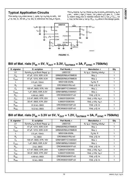
FIGURE 2. Typical Application Circuit
The first equation to calculate for any buck converter is duty-
cycle. Ignoring conduction losses associated with the FETs
and parasitic resistances it can be approximated by:
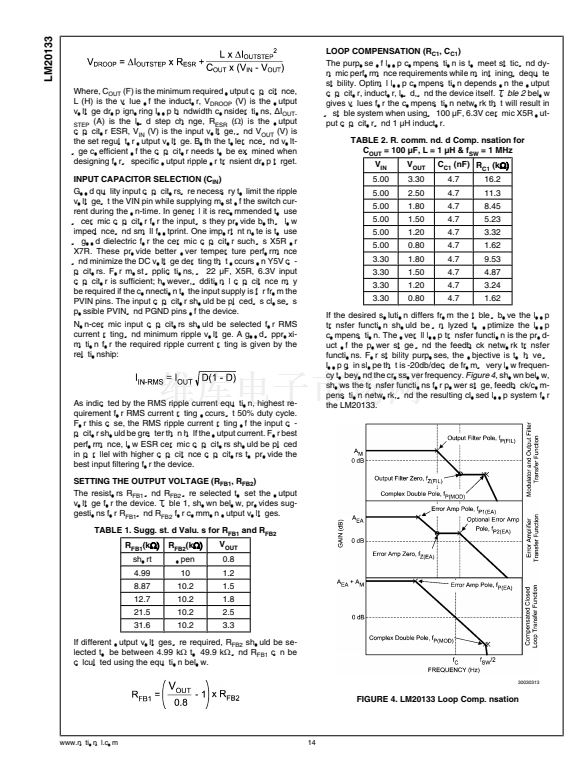
INDUCTOR SELECTION (L)
The inductor value is determined based on the operating fre-
quency, load current, ripple current, and duty cycle. The
inductor selected should have a saturation current rating
greater than the peak current limit of the device. Keep in mind
the specified current limit does not account for delay of the
current limit comparator, therefore the current limit in the ap-
plication may be higher than the specified value. To optimize
the performance and prevent the device from entering current
limit at maximum load, the inductance is typically selected
such that the ripple current,
螖i
L
, is less than 30% of the rated
output current.
Figure 3,
shown below illustrates the switch
and inductor ripple current waveforms. Once the input volt-
age, output voltage, operating frequency, and desired ripple
current are known, the minimum value for the inductor can be
calculated by the formula shown below:
Where,
螖V
OUT
(V) is the amount of peak to peak voltage ripple
at the power supply output, R
ESR
(鈩?
is the series resistance
of the output capacitor, f
SW
(Hz) is the switching frequency,
and C
OUT
(F) is the output capacitance used in the design.
The amount of output ripple that can be tolerated is applica-
tion specific; however a general recommendation is to keep
the output ripple less than 1% of the rated output voltage.
Keep in mind ceramic capacitors are sometimes preferred
because they have very low ESR; however, depending on
package and voltage rating of the capacitor the value of the
capacitance can drop significantly with applied voltage. The
output capacitor selection will also affect the output voltage
droop during a load transient. The peak droop on the output
voltage during a load transient is dependent on many factors;
however, a best case approximation of the transient droop
ignoring loop bandwidth can be obtained using the following
equation.
13
www.national.com


 1
1
 2
2
 3
3
 4
4
 5
5
 6
6
 7
7
 8
8
 9
9
 10
10
 11
11
 12
12
 13
13
 14
14
 15
15
 16
16
 17
17
 18
18
 19
19
 20
20
 21
21
 22
22
