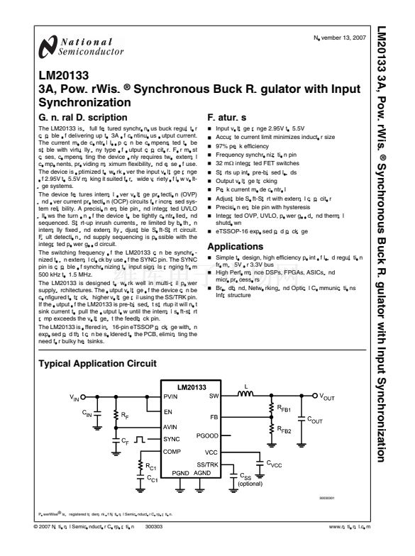
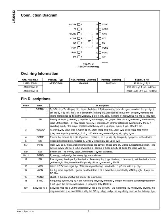
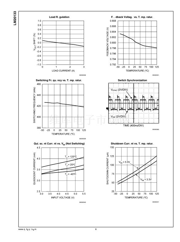
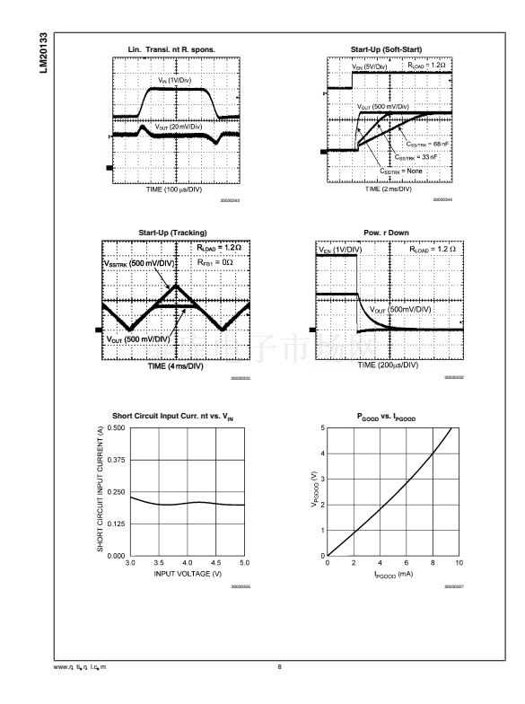
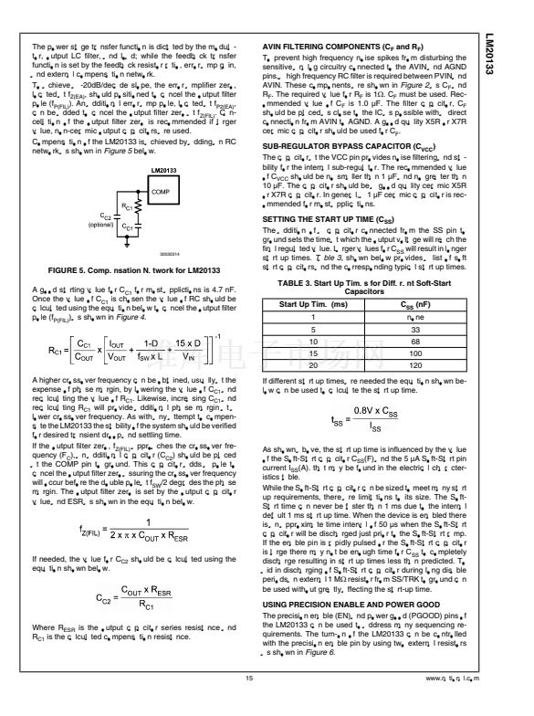
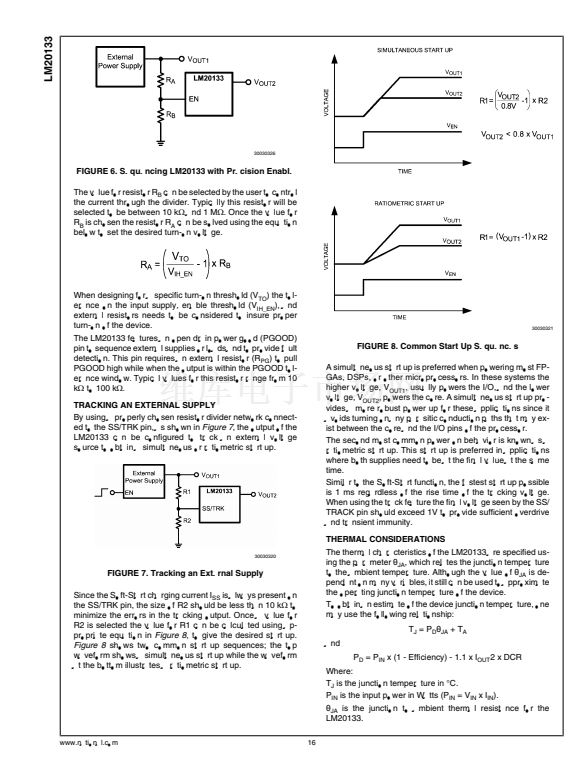
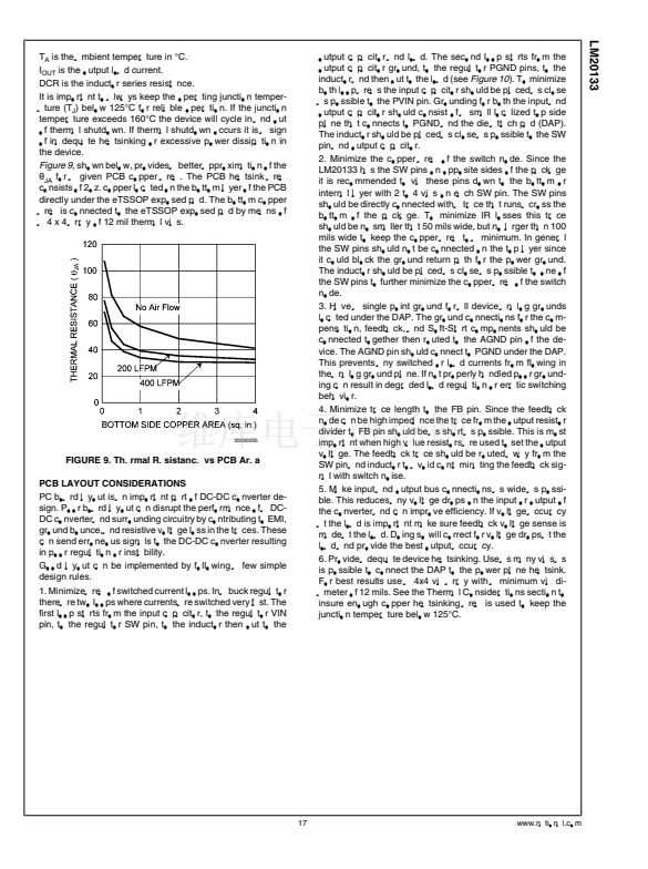
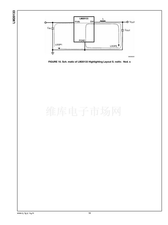
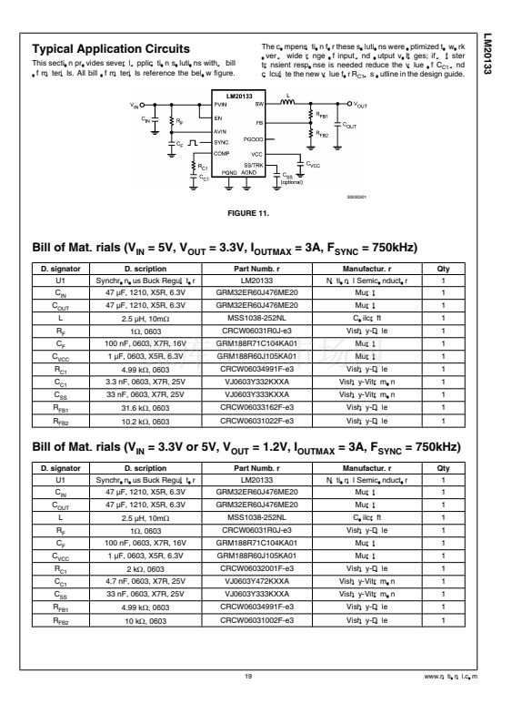
LM20133
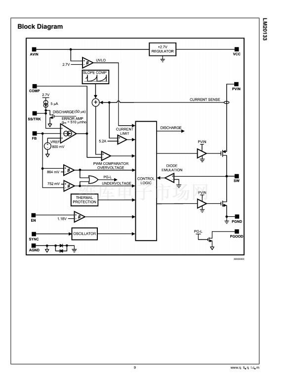
go low. Typical values for the PGOOD resistor are on the or-
der of 100 k鈩?or less. To avoid false tripping during transient
glitches the PGOOD pin has 16 碌s of built in deglitch time to
both rising and falling edges.
UVLO
The LM20133 has a built-in under-voltage lockout protection
circuit that keeps the device from switching until the input
voltage reaches 2.7V (typical). The UVLO threshold has 45
mV of hysteresis that keeps the device from responding to
power-on glitches during start up. If desired the turn-on point
of the supply can be changed by using the precision enable
pin and a resistor divider network connected to V
IN
as shown
in
Figure 6
in the design guide.
THERMAL PROTECTION
Internal thermal shutdown circuitry is provided to protect the
integrated circuit in the event that the maximum junction tem-
perature is exceeded. When activated, typically at 160擄C, the
LM20133 tri-states the power FETs and resets soft start. After
the junction cools to approximately 150擄C, the part starts up
using the normal start up routine. This feature is provided to
prevent catastrophic failures from accidental device over-
heating.
LIGHT LOAD OPERATION
The LM20133 offers increased efficiency when operating at
light loads. Whenever the load current is reduced to a point
where the inductor ripple current is greater than two times the
load current, the part will enter the diode emulation mode
preventing significant negative inductor current. The point at
which this occurs is the critical conduction boundary and can
be calculated by the following equation:
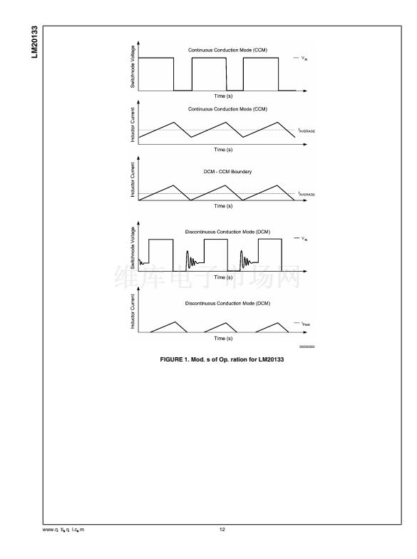
Several diagrams are shown in
Figure 1
illustrating continu-
ous conduction mode (CCM), discontinuous conduction
mode, and the boundary condition.
It can be seen that in diode emulation mode, whenever the
inductor current reaches zero the SW node will become high
impedance. Ringing will occur on this pin as a result of the LC
tank circuit formed by the inductor and the parasitic capaci-
tance at the node. If this ringing is of concern an additional
RC snubber circuit can be added from the switch node to
ground.
At very light loads, usually below 100 mA, several pulses may
be skipped in between switching cycles, effectively reducing
the switching frequency and further improving light-load effi-
ciency.
11
www.national.com


 1
1
 2
2
 3
3
 4
4
 5
5
 6
6
 7
7
 8
8
 9
9
 10
10
 11
11
 12
12
 13
13
 14
14
 15
15
 16
16
 17
17
 18
18
 19
19
 20
20
 21
21
 22
22
