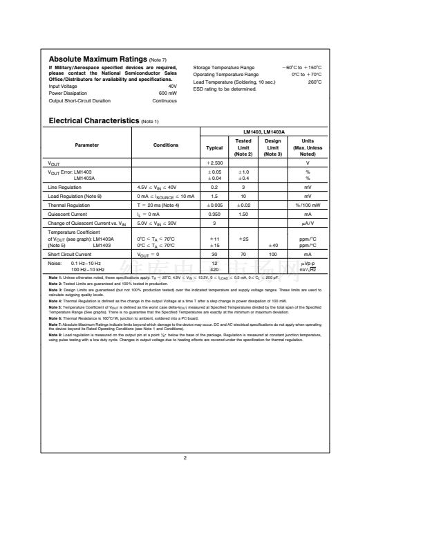
Absolute Maximum Ratings
(Note 7)
If Military Aerospace specified devices are required
please contact the National Semiconductor Sales
Office Distributors for availability and specifications
Input Voltage
Power Dissipation
Output Short-Circuit Duration
40V
600 mW
Continuous
Storage Temperature Range
Operating Temperature Range
Lead Temperature (Soldering 10 sec )
ESD rating to be determined
b
60 C to
a
150 C
0 C to
a
70 C
260 C
Electrical Characteristics
(Note 1)
LM1403 LM1403A
Parameter
Conditions
Typical
a
2 500
g
0 05
g
0 04
g
1 0
g
0 4
Tested
Limit
(Note 2)
Design
Limit
(Note 3)
Units
(Max Unless
Noted)
V
%
%
mV
mV
% 100 mW
mA
mA
V
V
OUT
V
OUT
Error LM1403
LM1403A
Line Regulation
Load Regulation (Note 8)
Thermal Regulation
Quiescent Current
Change of Quiescent Current vs V
IN
Temperature Coefficient
of V
OUT
(see graph) LM1403A
(Note 5)
LM1403
Short Circuit Current
Noise
0 1 Hz鈥?0 Hz
100 Hz鈥?0 kHz
4 5V
s
V
IN
s
40V
0 mA
s
I
SOURCE
s
10 mA
T
e
20 ms (Note 4)
I
L
e
0 mA
5 0V
s
V
IN
s
30V
0 C
s
T
A
s
70 C
0 C
s
T
A
s
70 C
V
OUT
e
0
02
15
g
0 005
3
10
g
0 02
0 350
3
g
11
g
15
1 50
g
25
g
40
ppm C
ppm C
mA
mVp-p
nV
0
Hz
30
12
420
70
100
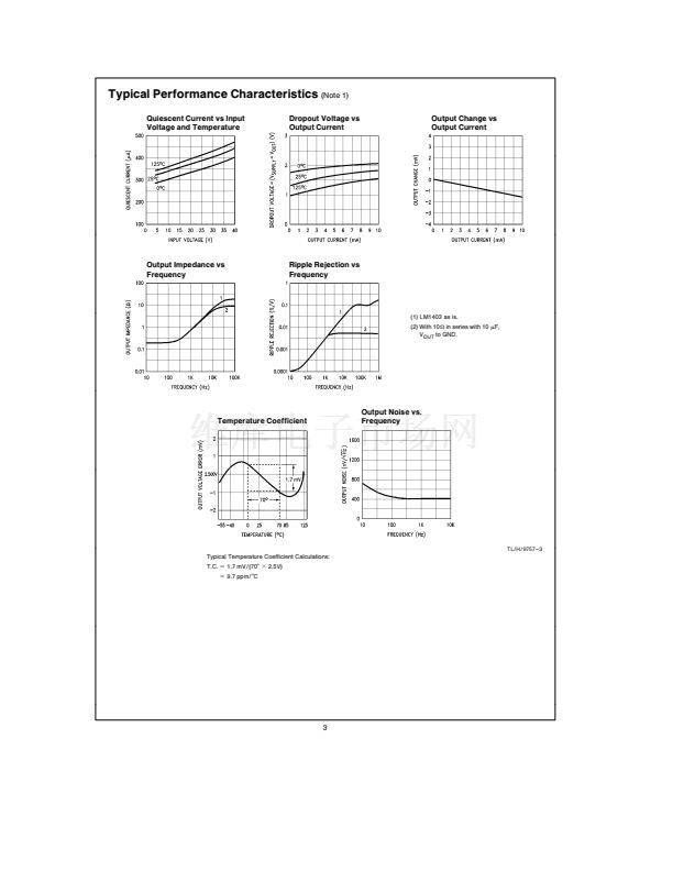
Note 1
Unless otherwise noted these specifications apply T
A
e
25 C 4 9V
s
V
IN
s
15 5V 0
s
I
LOAD
s
0 5 mA 0
s
C
L
s
200 pF
Note 2
Tested Limits are guaranteed and 100% tested in production
Note 3
Design Limits are guaranteed (but not 100% production tested) over the indicated temperature and supply voltage ranges These limits are used to
calculate outgoing quality levels
Note 4
Thermal Regulation is defined as the change in the output Voltage at a time T after a step change in power dissipation of 100 mW
Note 5
Temperature Coefficient of V
OUT
is defined as the worst case delta-V
OUT
measured at Specified Temperatures divided by the total span of the Specified
Temperature Range (See graphs) There is no guarantee that the Specified Temperatures are exactly at the minimum or maximum deviation
Note 6
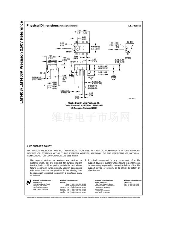
Thermal Resistance is 160 C W junction to ambient soldered into a PC board
Note 7
Absolute Maximum Ratings indicate limits beyond which damage to the device may occur DC and AC electrical specifications do not apply when operating
the device beyond its Rated Operating Conditions (see Note 1 and Conditions)
Note 8
Load regulation is measured on the output pin at a point
below the base of the package Regulation is measured at constant junction temperature
using pulse testing with a low duty cycle Changes in output voltage due to heating effects are covered under the specification for thermal regulation
2


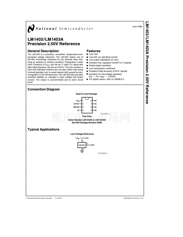 1
1
 2
2
 3
3
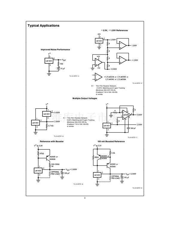 4
4
 5
5
 6
6
