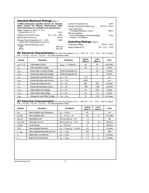
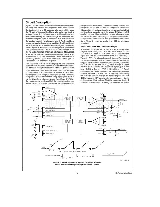
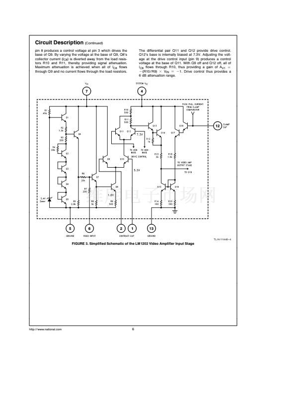
Circuit Description
(Continued)
VIDEO AMPLIFIER SECTION (Output Stage)
A simplified schematic of LM1202鈥檚 video amplifier output
stage is shown in
Figure 4
The output stage is the second
gain stage Ideally the gain of the second gain stage would
be A
V2
e b
R21 R18
e b
16 Because of the output
stage鈥檚 low open loop gain the gain is approximately
A
V2
e b
10 Thus the maximum gain of the video amplifier
is A
V
e
A
V1
c
A
V2
e
20 Transistors Q23 and Q24 provide
a push-pull drive to the load The output voltage can swing
from 0 2V to 10V
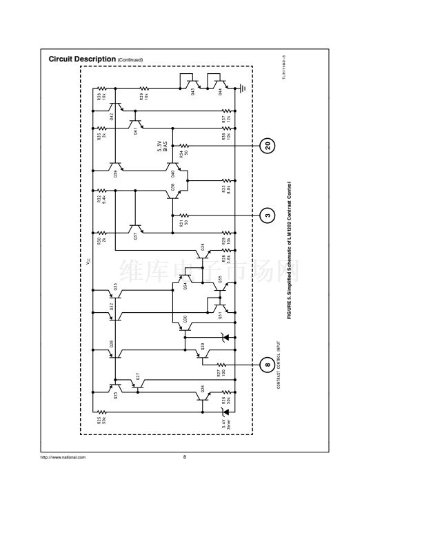
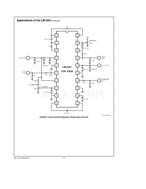
CONTRAST CONTROL SECTION
A simplified schematic of LM1202鈥檚 contrast control section
is shown in
Figure 5
A 0V to 4V DC voltage is applied at the
contrast input (pin 8) Transistors Q29 Q30 and Q34 buffer
and level shift the contrast voltage to the base of Q36 The
voltage at the emitter of Q36 equals the contrast voltage
(V
cont
) and the current through Q36鈥檚 collector is given by
I
C36
e
V
cont
R28
Transistor Q36鈥檚 collector current is used to unbalance the
current through the differential pair comprised of Q38
and Q40 Q40鈥檚 base is internally biased at 5 3V and made
available at pin 20 Pin 20 is externally connected to pin 1
through a 100X resistor (see
Figures 2
and
3
) The base of
Q38 (pin 3) is externally connected to pin 2 through a 100X
resistor (see
Figures 2
and
3
) With V
cont
e
2V the differ-
ential pair (Q38 Q40) is balanced and the voltage at pins 1
and 2 is 5 3V Under this condition Q8鈥檚 collector current is
equally split between Q9 and Q10 (see
Figure 3
) and the
amplifier鈥檚 gain is half the maximum gain If contrast voltage
at pin 8 is greater than 2V then Q36鈥檚 collector current
increases thus pulling Q38鈥檚 collector node lower and
consequently moving Q38鈥檚 base below 5 3V With pin 2
at a lower voltage than pin 1 current through Q10 (see
Figure 3
) increases and the amplifier鈥檚 gain increases With
V
cont
e
4V the amplifier鈥檚 gain is maximum
If the contrast voltage at pin 8 is less than 2V then Q36鈥檚
collector current decreases and Q38鈥檚 base is pulled above
5 3V With pin 2 voltage greater than pin 1 voltage less
current flows through Q10 (see
Figure 3
) consequently the
amplifier鈥檚 gain decreases With V
cont
e
0V the amplifier鈥檚
gain is minimum (i e maximum attenuation)
TL H 11440 鈥?
FIGURE 4 Simplified Schematic of LM1202 Video Amplifier Output Stage
7
http
www national com


 1
1
 2
2
 3
3
 4
4
 5
5
 6
6
 7
7
 8
8
 9
9
 10
10
 11
11
 12
12
 13
13
 14
14
 15
15
 16
16
 17
17
 18
18
