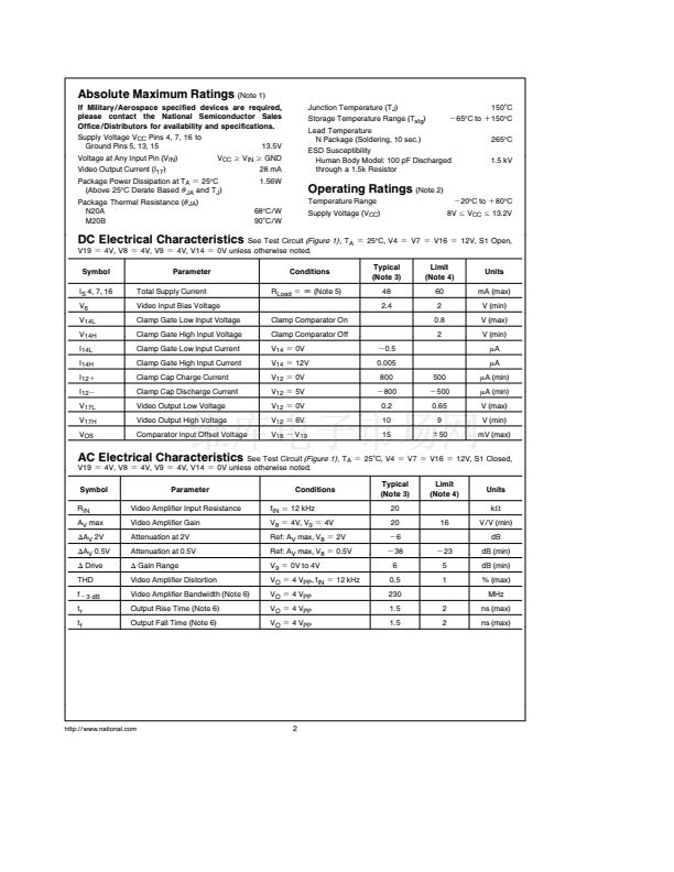
Circuit Description
Figure 2
shows a block diagram of the LM1202 video ampli-
fier along with contrast and brightness (black level) control
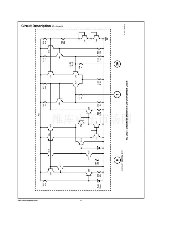
Contrast control is a DC-operated attenuator which varies
the AC gain of the amplifier Signal attenuation (contrast) is
achieved by varying the base drive to a differential pair and
thereby unbalancing the current through the differential pair
As shown in
Figure 2
pin 20 provides a 5 3V bias voltage for
the positive input of the attenuator (pin 1) Pin 3 provides a
control voltage for the negative input (pin 2) of the attenua-
tor The voltage at pin 3 varies as the voltage at the contrast
control input (pin 8) varies thus providing signal attenuation
The gain is maximum (0 dB attenuation) if the voltage at pin
8 is 4V and is minimum (maximum attenuation) if the voltage
at pin 8 is 0V The 0V to 4V DC-operated drive control at pin
9 provides a 6 dB gain adjustment range This feature is
necessary for RGB applications where independent gain ad-
justment of each channel is required
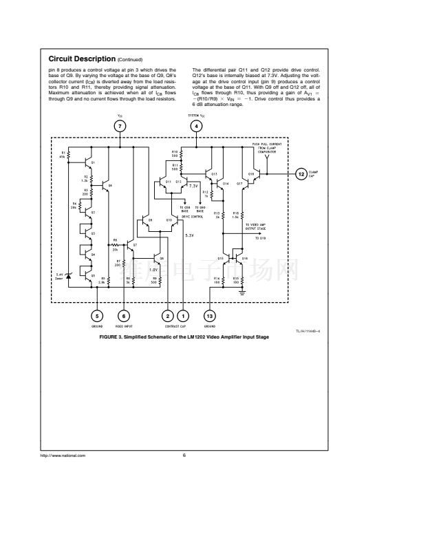
The brightness or black level clamping requires a 鈥樷€榮ample
and hold鈥欌€?circuit which holds the DC bias of the video ampli-
fier constant during the black level reference portion of the
video waveform Black level clamping often referred to as
DC restoration is accomplished by applying a back porch
clamp signal to the clamp gate input pin (pin 14) The clamp
comparator is enabled when the clamp signal goes low dur-
ing the black level reference period (see
Figure 2
) When
the clamp comparator is enabled the clamp capacitor con-
nected to pin 12 is either charged or discharged until the
voltage at the minus input of the comparator matches the
voltage set at the plus input of the comparator During the
video portion of the signal the clamp comparator is disabled
and the clamp capacitor holds the proper DC bias In a DC
coupled cathode drive application picture brightness func-
tion can be achieved by varying the voltage at the compara-
tor鈥檚 plus input Note that the back porch clamp pulse width
(t
W
in
Figure 2
) must be greater than 100 ns for proper
operation
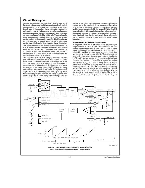
VIDEO AMPLIFIER SECTION (Input Stage)
A simplified schematic of LM1202鈥檚 video amplifier input
stage is shown in
Figure 3
The 5 4V zener diode Q1 Q6
and R2 bias the base of Q7 at 2 6V The AC coupled video
signal applied to pin 6 is referenced to the 2 6V bias voltage
Transistor Q7 buffers the video signal V
IN
and Q8 converts
the voltage to current The AC collector current through Q8
is I
C8
e
V
IN
R9 Under maximum gain condition transistors
Q9 and Q11 are off and all of I
C8
flows through the load
resistors R10 and R11 The maximum signal gain at the
base of Q13 is A
V1
e b
(R10
a
R11) R9
e b
2 Signal
attenuation is achieved by varying the base drive to the dif-
ferential pairs Q9 Q10 and Q11 Q12 thereby unbalancing
the collector currents through the transistor pairs Base of
Q10 is biased at 5 3V by externally connecting pin 1 to pin
20 through a 100X resistor Pin 2 is connected to pin 3
through a 100X resistor Adjusting the contrast voltage at
TL H 11440 鈥?3
FIGURE 2 Block Diagram of the LM1202 Video Amplifier
with Contrast and Brightness (Black Level) Control
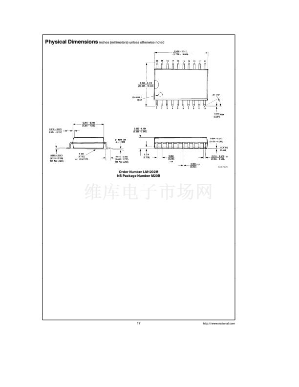
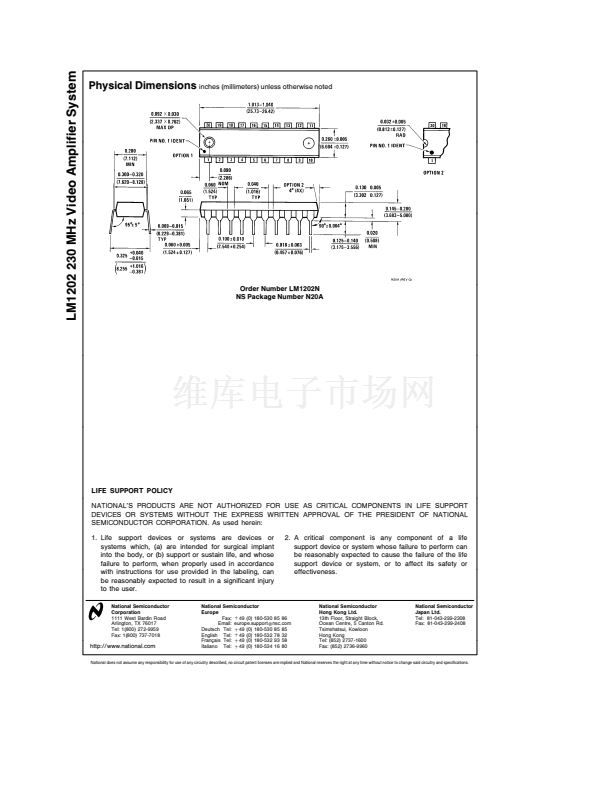
5
http
www national com


 1
1
 2
2
 3
3
 4
4
 5
5
 6
6
 7
7
 8
8
 9
9
 10
10
 11
11
 12
12
 13
13
 14
14
 15
15
 16
16
 17
17
 18
18
