鈥?/div>
PGND
SHDN
SV
IN
REF
AND
V
CC
V
REF
(1.19V)
V
CC
SGND
OPERATION
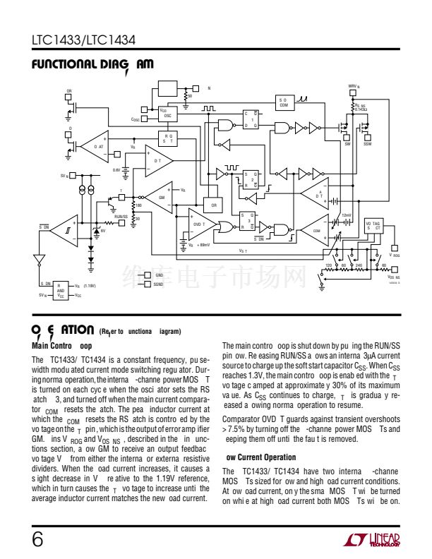
Main Control Loop
(Refer to Functional Diagram)
The LTC1433/LTC1434 is a constant frequency, pulse-
width modulated current mode switching regulator. Dur-
ing normal operation, the internal P-channel power MOSFET
is turned on each cycle when the oscillator sets the RS
latch FF3, and turned off when the main current compara-
tor I
COMP
resets the latch. The peak inductor current at
which the I
COMP
resets the RS latch is controlled by the
voltage on the I
TH
pin , which is the output of error amplifier
GM. Pins V
PROG
and V
OSENSE
, described in the Pin Func-
tions section, allow GM to receive an output feedback
voltage V
FB
from either the internal or external resistive
dividers. When the load current increases, it causes a
slight decrease in V
FB
relative to the 1.19V reference,
which in turn causes the I
TH
voltage to increase until the
average inductor current matches the new load current.
The main control loop is shut down by pulling the RUN/SS
pin low. Releasing RUN/SS allows an internal 3碌A(chǔ) current
source to charge up the soft start capacitor C
SS
. When C
SS
reaches 1.3V, the main control loop is enabled with the I
TH
voltage clamped at approximately 30% of its maximum
value. As C
SS
continues to charge, I
TH
is gradually re-
leased allowing normal operation to resume.
Comparator OVDET guards against transient overshoots
> 7.5% by turning off the P-channel power MOSFETs and
keeping them off until the fault is removed.
Low Current Operation
The LTC1433/LTC1434 have two internal P-channel
MOSFETs sized for low and high load current conditions.
At low load current, only the small MOSFET will be turned
on while at high load current both MOSFETs will be on.
6
鈥?/div>
30k
SB Q
FF3
RB Q
鈥?/div>
+
+
W
PLL
50k
SLOPE
COMP
V
CO
OSC
CK Q
FF1
D
Q
R
SENSE
0.143鈩?/div>
PLLIN
PWRV
IN
FREQ
SHIFT
BSW
SSW
U
U
U
+
LIDET
鈥?/div>
SB Q
FF2
RB Q
12mV
VOLTAGE
SELECT
V
PROG
120k
60k
240k
60k
V
OSENSE
1433/34 FD


 1
1
 2
2
 3
3
 4
4
 5
5
 6
6
 7
7
 8
8
 9
9
 10
10
 11
11
 12
12
 13
13
 14
14
 15
15
 16
16
 17
17
 18
18
 19
19
 20
20
