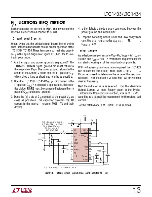
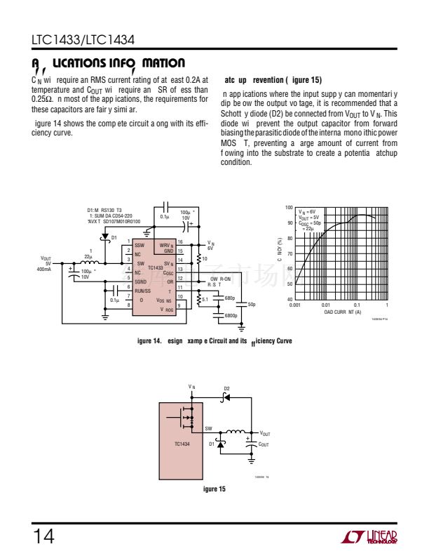
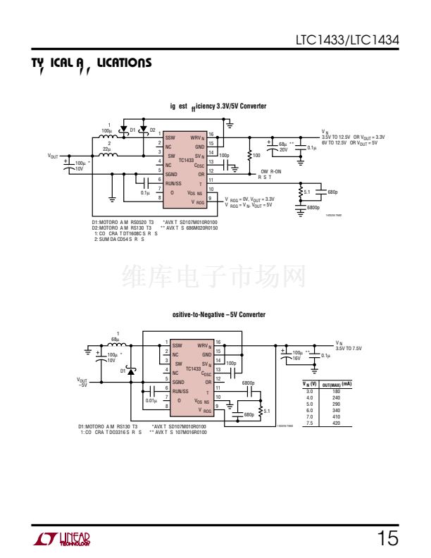
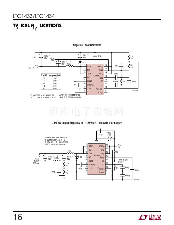
鈩?/div>
nA
nA
1.16
1.19
40
0.74
1
3.3
0.8
7
5
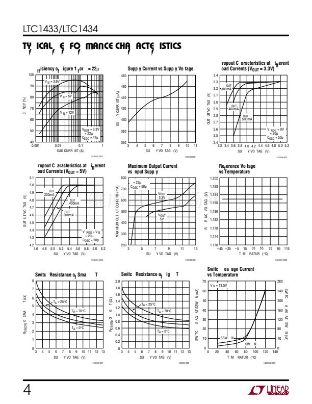
P-Channel Power FETs Characteristics
The
q
denotes specifications which apply over the specified temperature
range.
Note 1:
Absolute Maximum Ratings are those values beyond which the life
of a device may be impaired.
Note 2:
C-grade device specifications are guaranteed over the 0擄C to 70擄C
temperature range. In addition, C-grade device specifications are assured
over the 鈥?40擄C to 85擄C temperature range by design or correlation, but
are not production tested.
Note 3:
I-grade device specifications are guaranteed over the 鈥?40擄C to
85擄C temperature range by design, testing or correlation.
Note 4:
T
J
is calculated from the ambient temperature T
A
and power
dissipation P
D
according to the following formula:
LTC1433/LTC1434: T
J
= T
A
+ (P
D
)(150擄C/W)
Note 5:
The LTC1433/LTC1434 are tested in a feedback loop which servos
V
OSENSE
to the feedback point for the error amplifier (V
ITH
= 1.19V).
Note 6:
Dynamic supply current is higher due to the gate charge being
delivered at the switching frequency.
Note 7:
Oscillator frequency is tested by measuring the C
OSC
charge and
discharge currents and applying the formula:
8.4(10
8
)
1 + 1
鈥?
f
OSC
(kHz) = C
OSC
(pF) + 11 I
CHG
I
DIS
(
)(
)
3


 1
1
 2
2
 3
3
 4
4
 5
5
 6
6
 7
7
 8
8
 9
9
 10
10
 11
11
 12
12
 13
13
 14
14
 15
15
 16
16
 17
17
 18
18
 19
19
 20
20
