LTC1433/LTC1434
APPLICATIONS INFORMATION
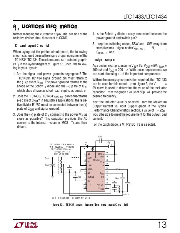
C
IN
will require an RMS current rating of at least 0.2A at
temperature and C
OUT
will require an ESR of less than
0.25鈩? In most of the applications, the requirements for
these capacitors are fairly similar.
Figure 14 shows the complete circuit along with its effi-
ciency curve.
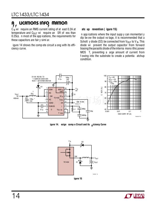
Latchup Prevention (Figure 15)
In applications where the input supply can momentarily
dip below the output voltage, it is recommended that a
Schottky diode (D2) be connected from V
OUT
to V
IN
. This
diode will prevent the output capacitor from forward
biasing the parasitic diode of the internal monolithic power
MOSFET, preventing a large amount of current from
flowing into the substrate to create a potential latchup
condition.
D1: MBRS130LT3
L1: SUMIDA CD54-220
*
AVX TPSD107M010R0100
D1
L1
22碌H
0.1碌F
1
2
3
4
5
6
SSW
NC
BSW
NC
PWRV
IN
PGND 15
SV
IN
C
OSC
POR
I
TH
V
OSENSE
V
PROG
14
13
12
11
10
9
16
V
IN
6V
10k
EFFICIENCY (%)
V
OUT
5V
400mA
+
100碌F*
10V
LTC1433
SGND
RUN/SS
LBO
LBI
0.1碌F
7
8
Figure 14. Design Example Circuit and its Efficiency Curve
LTC1434
14
U
W
U
U
100
100碌F*
10V
90
80
70
60
50
V
IN
= 6V
V
OUT
= 5V
C
OSC
= 50pF
L = 22碌H
+
POWER-ON
RESET
5.1k
680pF
50pF
6800pF
V
IN
D2
SW
D1
L
40
0.001
0.01
0.1
LOAD CURRENT (A)
1
1433/34 F14
+
V
OUT
C
OUT
1433/34 F15
Figure 15


 1
1
 2
2
 3
3
 4
4
 5
5
 6
6
 7
7
 8
8
 9
9
 10
10
 11
11
 12
12
 13
13
 14
14
 15
15
 16
16
 17
17
 18
18
 19
19
 20
20
