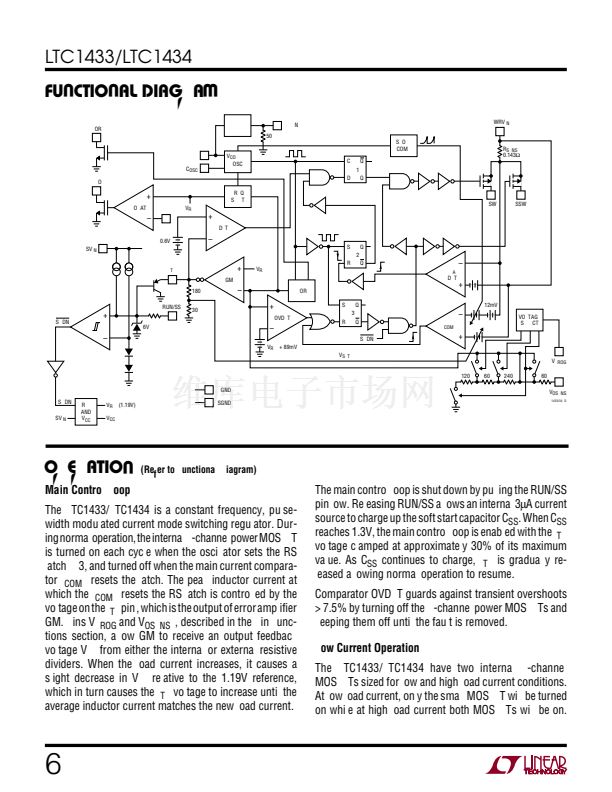
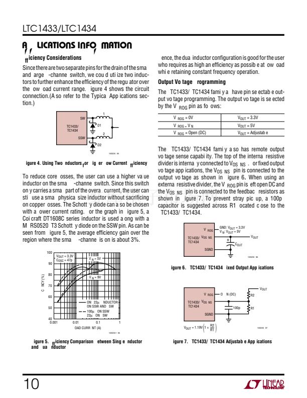
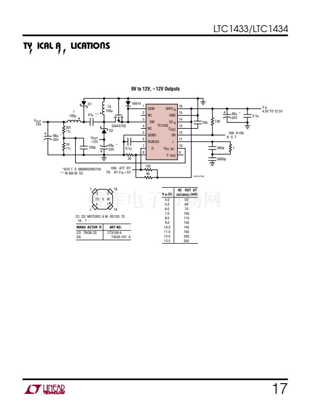
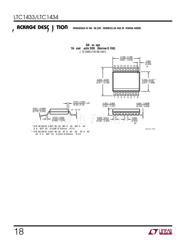
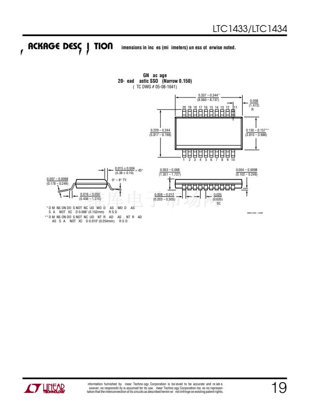
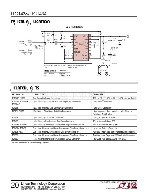
LTC1433/LTC1434
APPLICATIONS INFORMATION
further reducing the current to 15碌A(chǔ). The low side of the
resistive divider should connect to SGND.
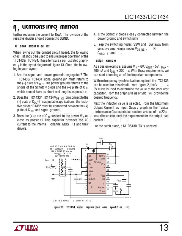
PC Board Layout Checklist
When laying out the printed circuit board, the following
checklist should be used to ensure proper operation of the
LTC1433/LTC1434. These items are also illustrated graphi-
cally in the layout diagram of Figure 13. Check the follow-
ing in your layout:
1. Are the signal and power grounds segregated? The
LTC1433/LTC1434 signal ground pin must return to
the (鈥? plate of C
OUT
. The power ground returns to the
anode of the Schottky diode and the (鈥? plate of C
IN
,
which should have as short lead lengths as possible.
2. Does the LTC1433/LTC1434 V
OSENSE
pin connect to the
(+) plate of C
OUT
? In adjustable applications, the resis-
tive divider R1/R2 must be connected between the (+)
plate of C
OUT
and signal ground.
3. Does the (+) plate of C
IN
connect to the power V
IN
as
close as possible? This capacitor provides the AC
current to the internal P-channel MOSFETs and their
drivers.
4. Is the Schottky diode closely connected between the
power ground and switch pin?
5. Keep the switching nodes, SSW and BSW away from
sensitive small-signal nodes V
OSENSE
, PLLIN, PLL LPF,
C
OSC
, I
TH
and LBI.
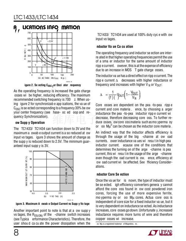
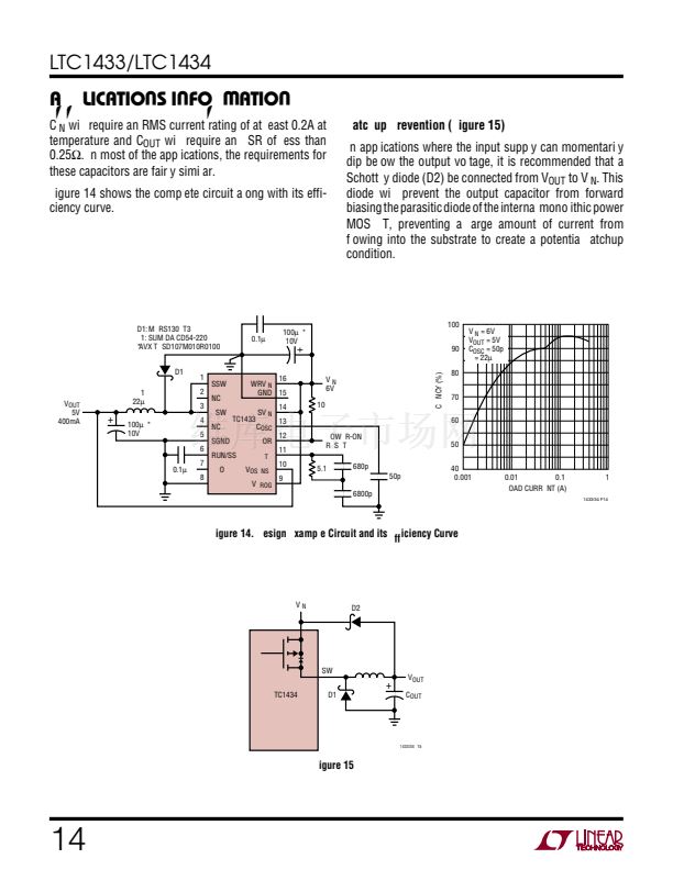
Design Example
As a design example, assume V
IN
= 6V, V
OUT
= 5V, I
MAX
=
400mA and f
OSC
= 200kHz. With these requirements we
can start choosing all of the important components.
With no frequency synchronization required, the LTC1433
can be used for this circuit. From Figure 2, the V
PLL LPF
=
0V curve is used to determine the value of the oscillator
capacitor. From the graph a value of 50pF will provide the
desired frequency.
Next the inductor value is selected. From the Maximum
Output Current vs Input Supply graph in the Typical
Performance Characteristics section, a value of L = 22碌H
would be able to meet the requirement for the output load
current.
For the catch diode, a MBRS130LT3 is selected.
OUTPUT DIVIDER REQUIRED
WITH ADJUSTABLE VERSION
ONLY. CONNECT V
OSENSE
TO V
OUT
FOR FIXED
OUTPUT VOLTAGE
L1
V
OUT
C
OUT
+
BOLD LINES INDICATE HIGH CURRENT PATHS
Figure 13. LTC1434 Layout Diagram (See Board Layout Check List)
U
W
U
U
0.1碌F
D1
C
IN
+
1
2
3
4
5
6
C
SS
7
8
9
10
NC
SSW
NC
BSW
SGND
NC
RUN/SS
NC
LBO
LBI
20
PWRV
IN
PGND 19
LTC1434
SV
IN
18
17
16
15
14
13
12
11
C
OSC
PLLIN
PLL LPF
C
OSC
POR
I
TH
V
OSENSE
V
PROG
1433/34 F13
13


 1
1
 2
2
 3
3
 4
4
 5
5
 6
6
 7
7
 8
8
 9
9
 10
10
 11
11
 12
12
 13
13
 14
14
 15
15
 16
16
 17
17
 18
18
 19
19
 20
20
