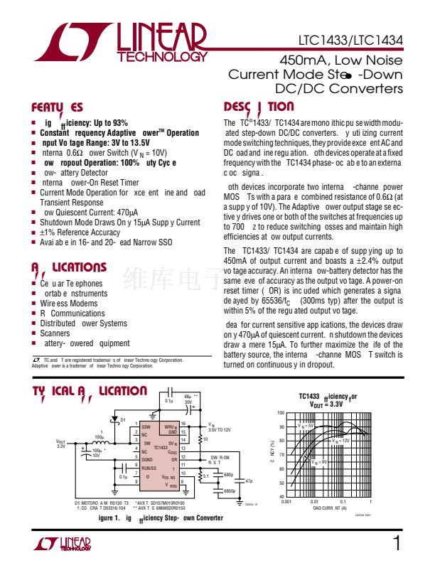
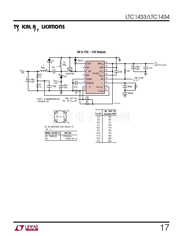
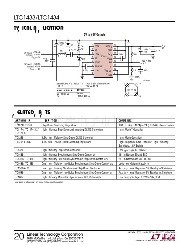
LTC1433/LTC1434
APPLICATIONS INFORMATION
1.3f
O
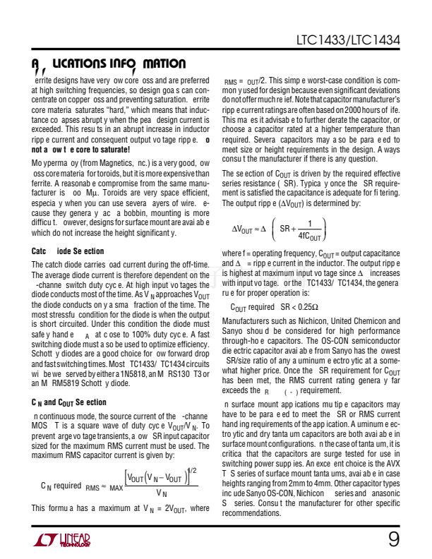
FREQUENCY (kHz)
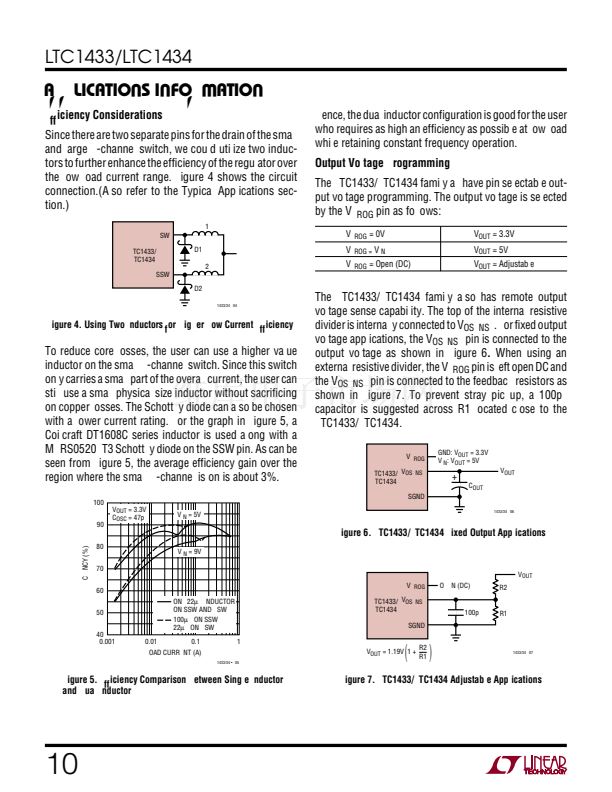
f
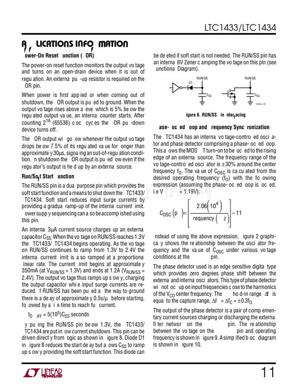
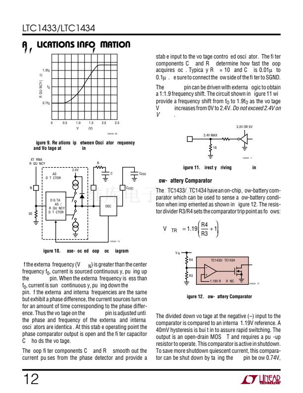
O
0.7f
O
0
0.5
1.0
1.5
V
PLLLPF
(V)
2.0
2.5
1433/34 F09
Figure 9. Relationship Between Oscillator Frequency
and Voltage at PLL LPF Pin
EXTERNAL
FREQUENCY
2.4V
PHASE
DETECTOR
PLLIN
PLL LPF
C
LP
R
LP
50k
DIGITAL
PHASE/
FREQUENCY
DETECTOR
OSC
1433/34 F10
Figure 10. Phase-Locked Loop Block Diagram
If the external frequency (V
PLLIN
) is greater than the center
frequency f
0
, current is sourced continuously, pulling up
the PLL LPF pin. When the external frequency is less than
f
0
, current is sunk continuously, pulling down the PLL LPF
pin. If the external and internal frequencies are the same
but exhibit a phase difference, the current sources turn on
for an amount of time corresponding to the phase differ-
ence. Thus the voltage on the PLL LPF pin is adjusted until
the phase and frequency of the external and internal
oscillators are identical. At this stable operating point the
phase comparator output is open and the filter capacitor
C
LP
holds the voltage.
The loop filter components C
LP
and R
LP
smooth out the
current pulses from the phase detector and provide a
12
U
W
U
U
stable input to the voltage controlled oscillator. The filter
components C
LP
and R
LP
determine how fast the loop
acquires lock. Typically R
LP
= 10k and C
LP
is 0.01碌F to
0.1碌F. Be sure to connect the low side of the filter to SGND.
The PLL LPF pin can be driven with external logic to obtain
a 1:1.9 frequency shift. The circuit shown in Figure 11 will
provide a frequency shift from f
O
to 1.9f
O
as the voltage
V
PLL LPF
increases from 0V to 2.4V.
Do not exceed 2.4V on
V
PLL LPF
.
3.3V OR 5V
PLL LPF
2.4V MAX
18k
1433/34 F11
Figure 11. Directly Driving PLL LPF Pin
C
OSC
Low-Battery Comparator
C
OSC
The LTC1433/LTC1434 have an on-chip, low-battery com-
parator which can be used to sense a low-battery condi-
tion when implemented as shown in Figure 12. The resis-
tor divider R3/R4 sets the comparator trip point as follows:
錚?/div>
R4
錚?/div>
V
LBTRIP
=
1.19
錚?/div>
+
1
錚?/div>
R3
錚?/div>
錚?/div>
V
IN
R4
LTC1433/LTC1434
鈥?/div>
R3
+
1.19V REFERENCE
1433/34 F12
Figure 12. Low-Battery Comparator
The divided down voltage at the negative (鈥? input to the
comparator is compared to an internal 1.19V reference. A
40mV hysteresis is built in to assure rapid switching. The
output is an open-drain MOSFET and requires a pull-up
resistor to operate. This comparator is active in shutdown.
To save more shutdown quiescent current, this compara-
tor can be shut down by taking the LBI pin below 0.74V,
LTC1433I PDF文件相關(guān)型號(hào)
LTC1434I
LTC1433I相關(guān)型號(hào)PDF文件下載
-
型號(hào)
版本
描述
廠商
下載
-
英文版
Dual Micropower Comparator
LINER
-
英文版
DUAL MICROPOWER COMPARATOR
LINER [Lin...
-
英文版
Dual Micropower Comparator
LINER [Lin...
-
英文版
BANG-BANG Controller
LINER
-
英文版
BANG-BANG Controller
LINER [Lin...
-
英文版
Window Comparator
LINER
-
英文版
Window Comparator
LINER [Lin...
-
英文版
Window Comparator
LINER [Lin...
-
英文版
2-Channel Differential Input 16-Bit No Latency DS ADC
LINER
-
英文版
2-Channel Differential Input 24-Bit No Latency DS ADC
LINER [Lin...
-
英文版
2-Channel Differential Input 16-Bit No Latency DS ADC
LINER [Lin...
-
英文版
Dual Precision Intrumentation Switched-Capacitor Building Bl...
LINER [Lin...
-
英文版
Switched Capacitor Voltage Converter
LINER
-
英文版
Switched Capacitor Voltage Converter
LINER [Lin...
-
英文版
Programmable Micropower Hex Translator/ Receiver/Driver
LINER
-
英文版
Programmable Micropower Hex Translator/ Receiver/Driver
LINER [Lin...
-
英文版
“Inductorless” 5V to + 5V Converter
LINER
-
英文版
“Inductorless” 5V to + 5V Converter
LINER [Lin...
-
英文版
Dual Micropower Chopper Stabilized Operational Amplifier wit...
LINER
-
英文版
Dual Micropower Zero-Drift Operational Amplifier with Intern...
LINER [Lin...


 1
1
 2
2
 3
3
 4
4
 5
5
 6
6
 7
7
 8
8
 9
9
 10
10
 11
11
 12
12
 13
13
 14
14
 15
15
 16
16
 17
17
 18
18
 19
19
 20
20
