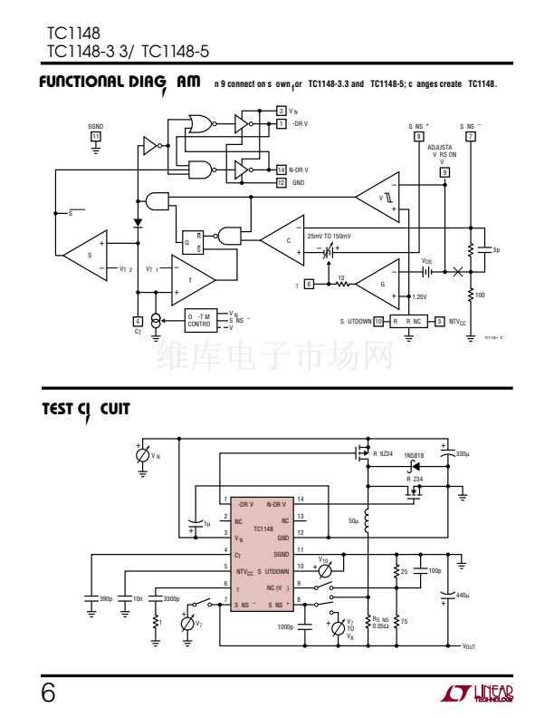
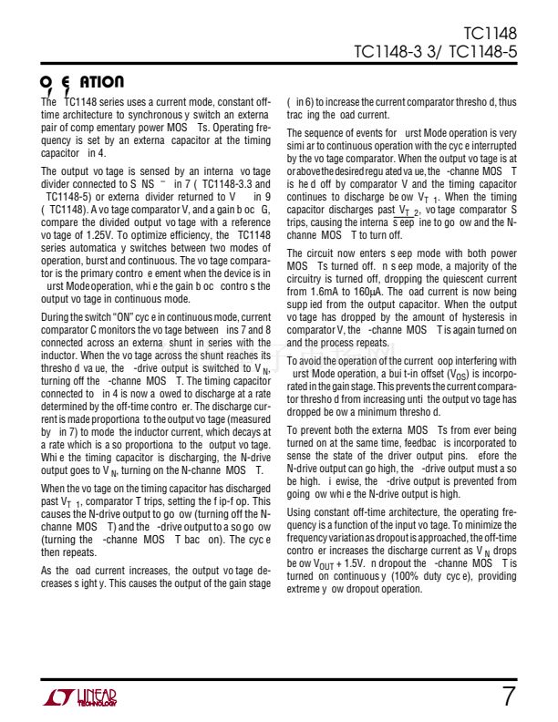
pair of complementary power MOSFETs. Operating fre-
capacitor Pin 4.
鈥?/div>
Pin 7 (LTC1148-3.3 and
LTC1148-5) or external divider returned to V
FB
Pin 9
(LTC1148). A voltage comparator V, and a gain block G,
compare the divided output voltage with a reference
voltage of 1.25V. To optimize efficiency, the LTC1148
series automatically switches between two modes of
operation, burst and continuous. The voltage compara-
tor is the primary control element when the device is in
Burst Mode operation, while the gain block controls the
output voltage in continuous mode.
During the switch 鈥淥N鈥?cycle in continuous mode, current
comparator C monitors the voltage between Pins 7 and 8
connected across an external shunt in series with the
inductor. When the voltage across the shunt reaches its
threshold value, the P-drive output is switched to V
IN
,
turning off the P-channel MOSFET. The timing capacitor
connected to Pin 4 is now allowed to discharge at a rate
determined by the off-time controller. The discharge cur-
rent is made proportional to the output voltage (measured
by Pin 7) to model the inductor current, which decays at
a rate which is also proportional to the output voltage.
While the timing capacitor is discharging, the N-drive
output goes to V
IN
, turning on the N-channel MOSFET.
When the voltage on the timing capacitor has discharged
past V
TH1
, comparator T trips, setting the flip-flop. This
causes the N-drive output to go low (turning off the N-
channel MOSFET) and the P-drive output to also go low
(turning the P-channel MOSFET back on). The cycle
then repeats.
As the load current increases, the output voltage de-
creases slightly. This causes the output of the gain stage
U
(Pin 6) to increase the current comparator threshold, thus
tracking the load current.
The sequence of events for Burst Mode operation is very
similar to continuous operation with the cycle interrupted
by the voltage comparator. When the output voltage is at
or above the desired regulated value, the P-channel MOSFET
is held off by comparator V and the timing capacitor
continues to discharge below V
TH1
. When the timing
capacitor discharges past V
TH2
, voltage comparator S
trips, causing the internal sleep line to go low and the N-
channel MOSFET to turn off.
The circuit now enters sleep mode with both power
MOSFETs turned off. In sleep mode, a majority of the
circuitry is turned off, dropping the quiescent current
from 1.6mA to 160碌A(chǔ). The load current is now being
supplied from the output capacitor. When the output
voltage has dropped by the amount of hysteresis in
comparator V, the P-channel MOSFET is again turned on
and the process repeats.
To avoid the operation of the current loop interfering with
Burst Mode operation, a built-in offset (V
OS
) is incorpo-
rated in the gain stage. This prevents the current compara-
tor threshold from increasing until the output voltage has
dropped below a minimum threshold.
To prevent both the external MOSFETs from ever being
turned on at the same time, feedback is incorporated to
sense the state of the driver output pins. Before the
N-drive output can go high, the P-drive output must also
be high. Likewise, the P-drive output is prevented from
going low while the N-drive output is high.
Using constant off-time architecture, the operating fre-
quency is a function of the input voltage. To minimize the
frequency variation as dropout is approached, the off-time
controller increases the discharge current as V
IN
drops
below V
OUT
+ 1.5V. In dropout the P-channel MOSFET is
turned on continuously (100% duty cycle), providing
extremely low dropout operation.
7


 1
1
 2
2
 3
3
 4
4
 5
5
 6
6
 7
7
 8
8
 9
9
 10
10
 11
11
 12
12
 13
13
 14
14
 15
15
 16
16
 17
17
 18
18
 19
19
 20
20
