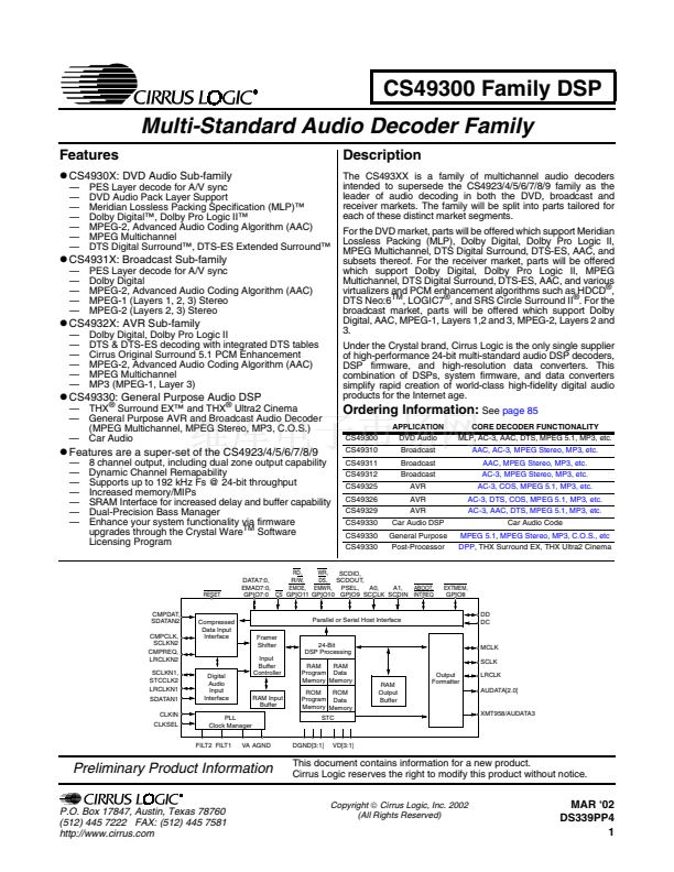
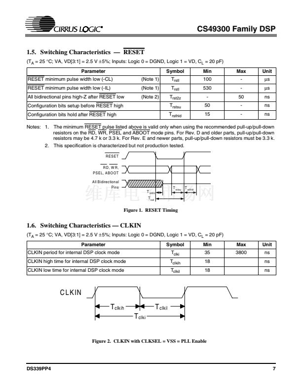
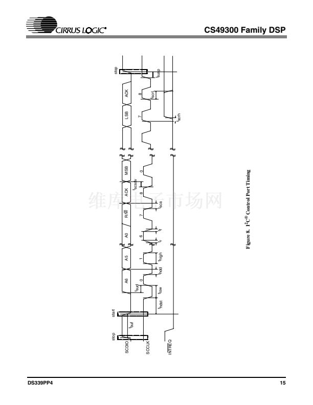
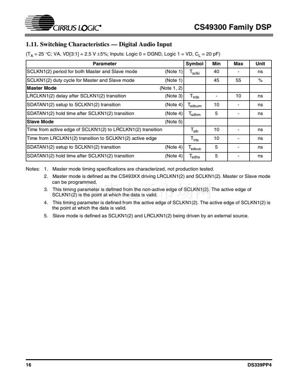
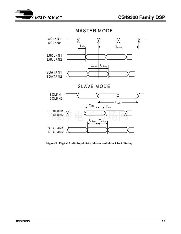
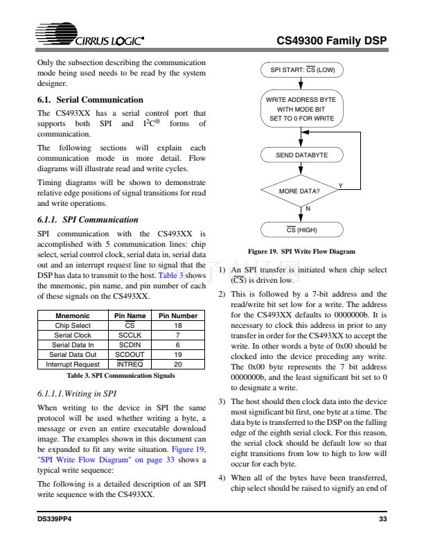
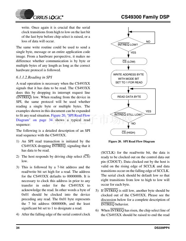
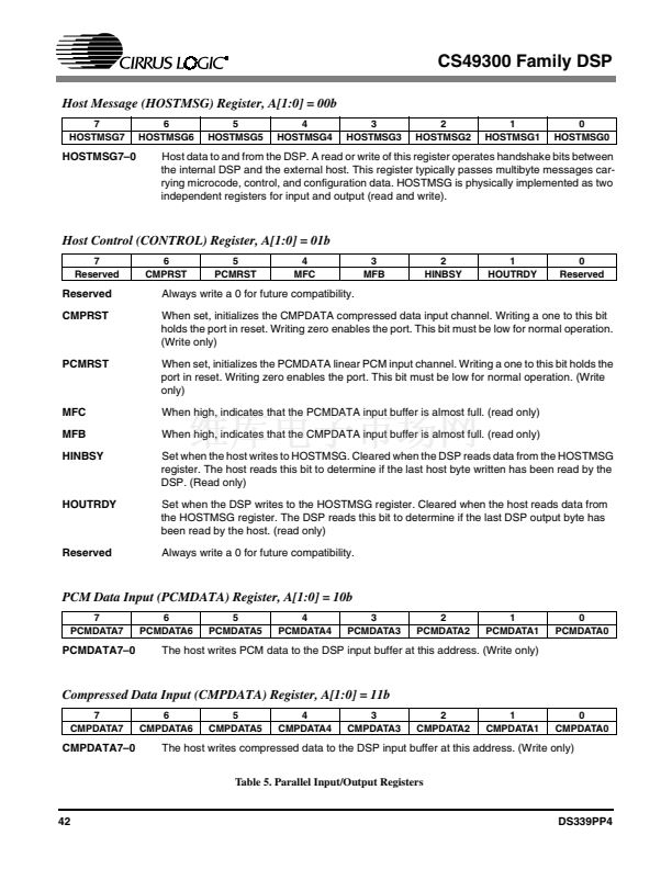
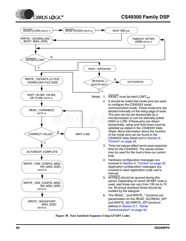
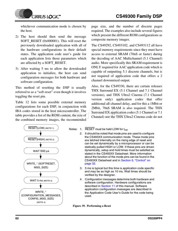
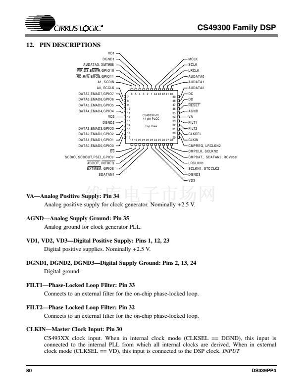
CS49300 Family DSP
During delivery of a block of data the FIFO
threshold should not be checked. In other words the
FIFO indicators are level sensitive and indicate that
a block can be delivered when they are low. They
may return high during the data delivery. When this
happens there is still room for the remaining bytes
of the block.
The PCM data input register (PCMDAT) receives
bytes of data when the host interface writes to
address 10b (A1 high, A0 low). The MFC bit in the
Host Control Register is an indicator of the PCM
FIFO level. The MFC bit remains low until the
FIFO threshold has been reached.
The PCMRST bit of the CONTROL register
provides
absolute
software/hardware
synchronization by initializing the input channel to
uniquely recognize the first write to the byte-wide
PCMDATA port. Toggling PCMRST high and low
informs the DSP that the next sample read from the
PCMDATA port is the first sample of the left
channel. In this fashion, the CS493XX can
translate successive byte writes into a variable
number of channels with a variable PCM sample
size. In the most simple case, the CS493XX can
receive stereo 8-bit PCM one byte at a time with the
internal DSP assigning the first 8-bit write (after
PCMRST) to the left channel and the second 8-bit
write to the right channel. For 24-bit PCM, it
assigns the first three 8-bit writes (after PCMRST)
to the left channel and the next three writes to the
right channel. Before starting PCM transfer, or to
initiate a new PCM transfer, the PCMRST bit must
be toggled as described above to insure data
integrity.
Data must be delivered to the CS493XX in blocks
of data. The block size is set through a hardware
configuration message. Before each block is
delivered, the host should check the MFC bit. If the
MFC bit is low, then the host can deliver a block of
data one byte at a time. If the MFC bit is high, no
more data should be sent to the CS493XX. Once
the MFC bit has gone low again, the host may send
another block of PCM audio data. The MFC bit is
FIFO level sensitive. In other words, it may change
during the transfer of a block. The host should
complete the block transfer and ignore the MFC bit
until the block transfer is complete.
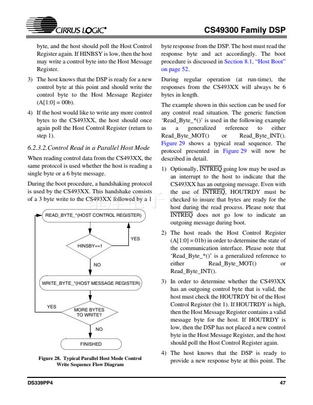
10.4.2.Parallel Delivery with Serial Control
When using I
2
C or SPI control, bytewide delivery
of data can still be achieved using
SCLKN2(CMPCLK) and GPIO[8:0]. In this mode
the bytewide parallel data is clocked into the part
on the transition of CMPCLK.
In this mode CMPREQ can be used as the FIFO
threshold indicator. When CMPREQ is low it
means that the CS493XX can receive another block
of data.
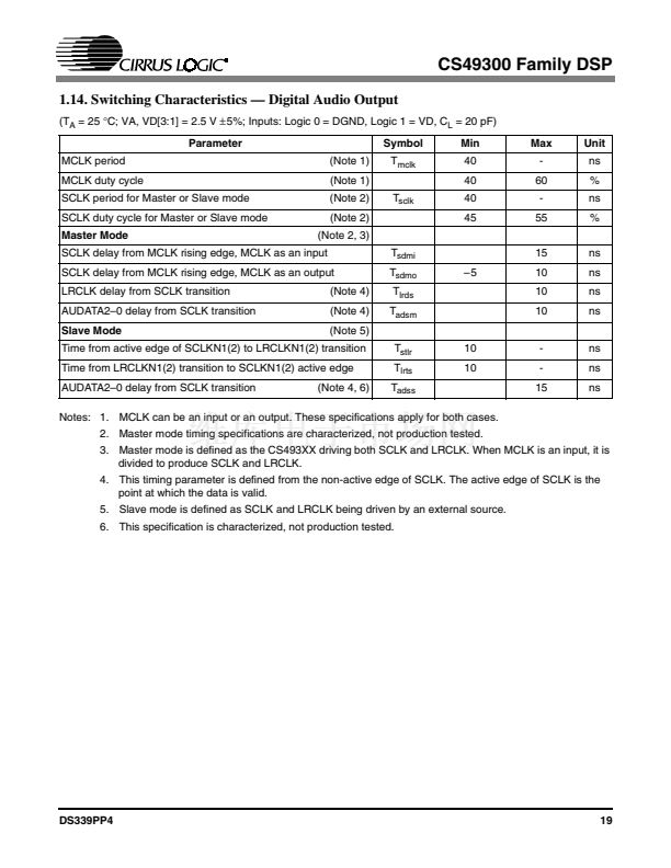
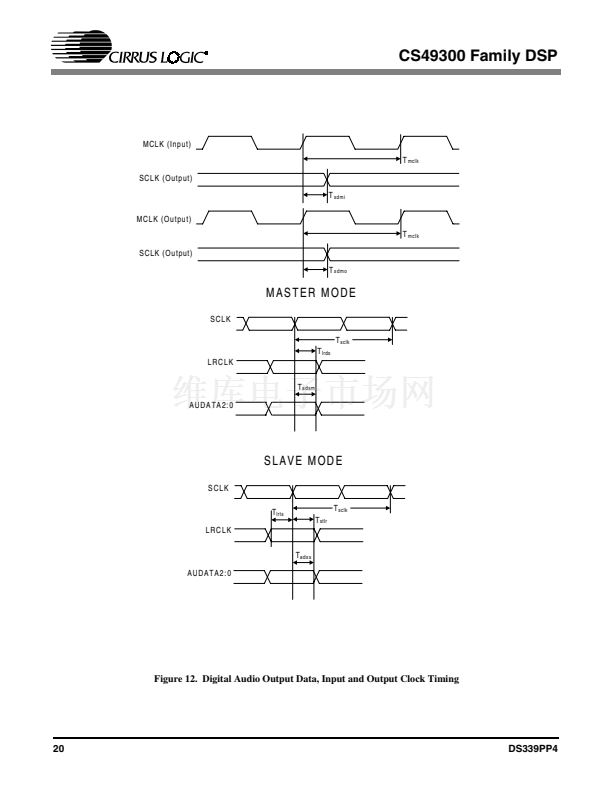
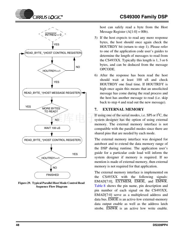
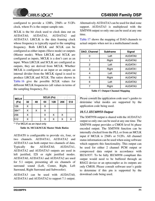
10.5. Digital Audio Output Port
The Digital Audio Output port, or DAO, is the port
used for digital output from the DSP.
Table 15
shows the signals associated with the DAO. As
with the input ports the clocks and data are fully
configurable via hardware configuration.
Pin Name
AUDATA3,
XMT958
AUDATA2
AUDATA1
AUDATA0
LRCLK
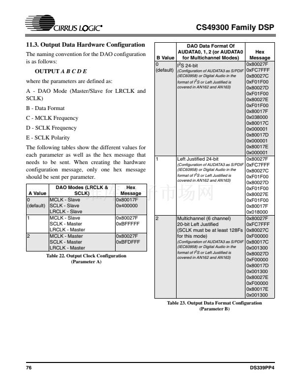
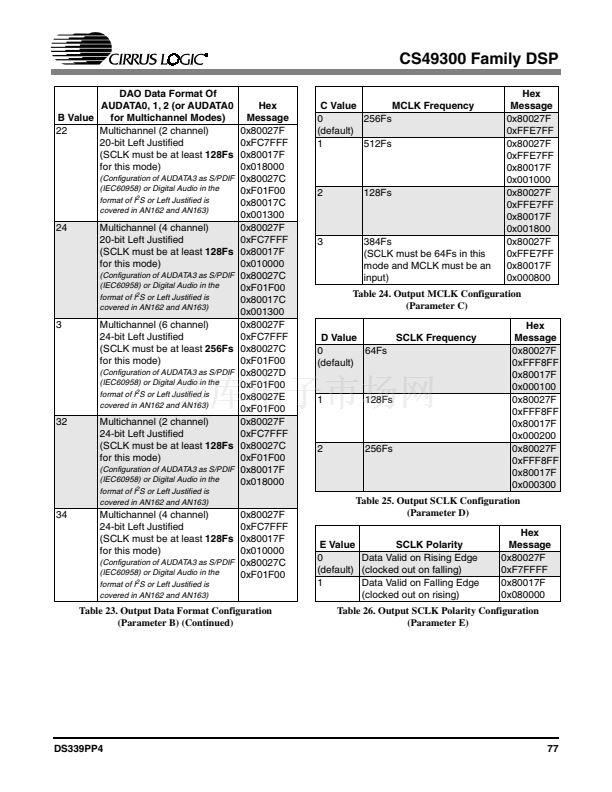
SCLK
MCLK
Pin Description
Serial Data Out
IEC60958 Transmitter
Serial Data Out
Serial Data Out
Serial Data Out
Frame Clock
Serial Bit Clock
Master Clock
Table 15. Digital Audio Output Port
Pin Number
3
39
40
41
42
43
44
MCLK is the master clock and is firmware
configurable to be either an input or an output. If
MCLK is to be used as an output, the internal PLL
must be used. As an output MCLK can be
70
DS339PP4


 1
1
 2
2
 3
3
 4
4
 5
5
 6
6
 7
7
 8
8
 9
9
 10
10
 11
11
 12
12
 13
13
 14
14
 15
15
 16
16
 17
17
 18
18
 19
19
 20
20
 21
21
 22
22
 23
23
 24
24
 25
25
 26
26
 27
27
 28
28
 29
29
 30
30
 31
31
 32
32
 33
33
 34
34
 35
35
 36
36
 37
37
 38
38
 39
39
 40
40
 41
41
 42
42
 43
43
 44
44
 45
45
 46
46
 47
47
 48
48
 49
49
 50
50
 51
51
 52
52
 53
53
 54
54
 55
55
 56
56
 57
57
 58
58
 59
59
 60
60
 61
61
 62
62
 63
63
 64
64
 65
65
 66
66
 67
67
 68
68
 69
69
 70
70
 71
71
 72
72
 73
73
 74
74
 75
75
 76
76
 77
77
 78
78
 79
79
 80
80
 81
81
 82
82
 83
83
 84
84
 85
85
 86
86
