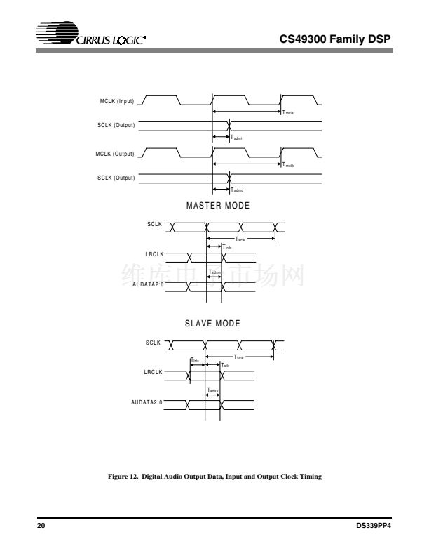
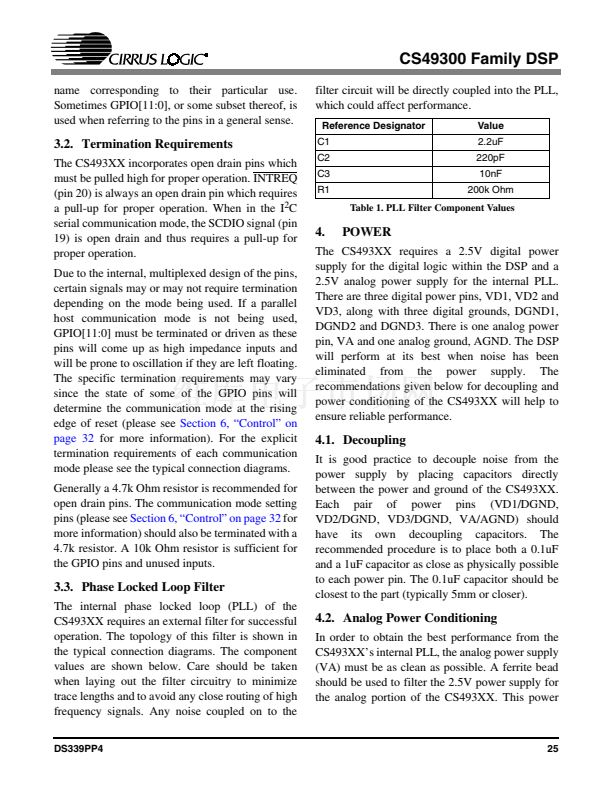
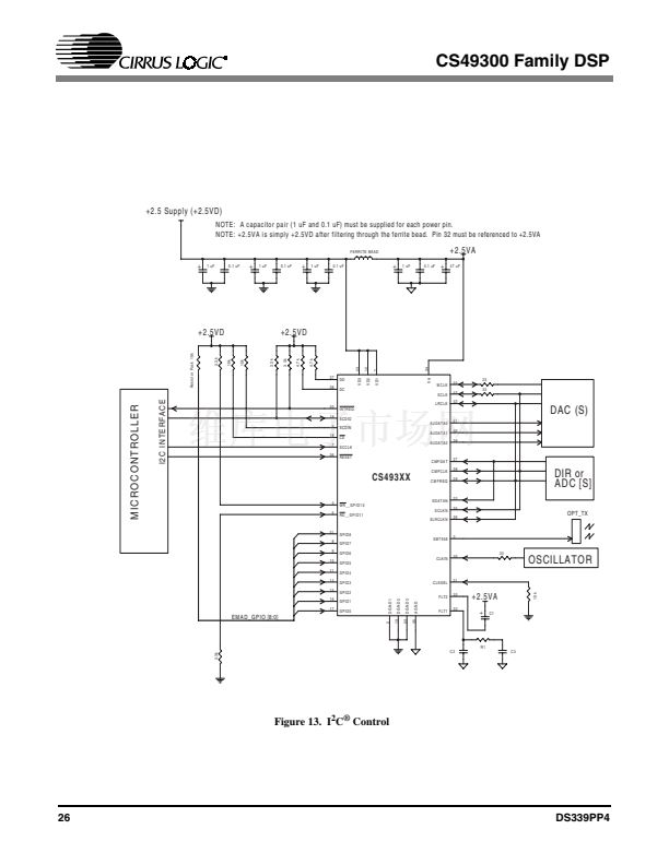
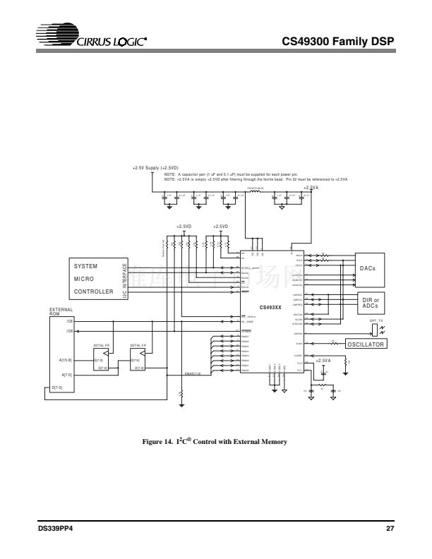
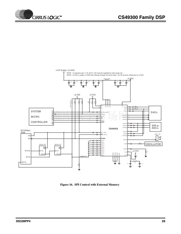
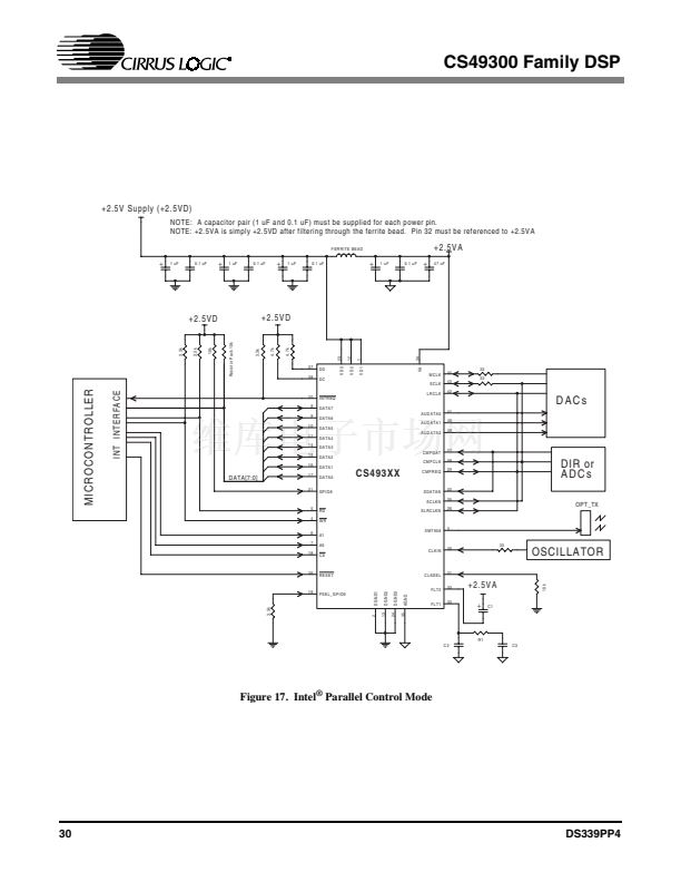
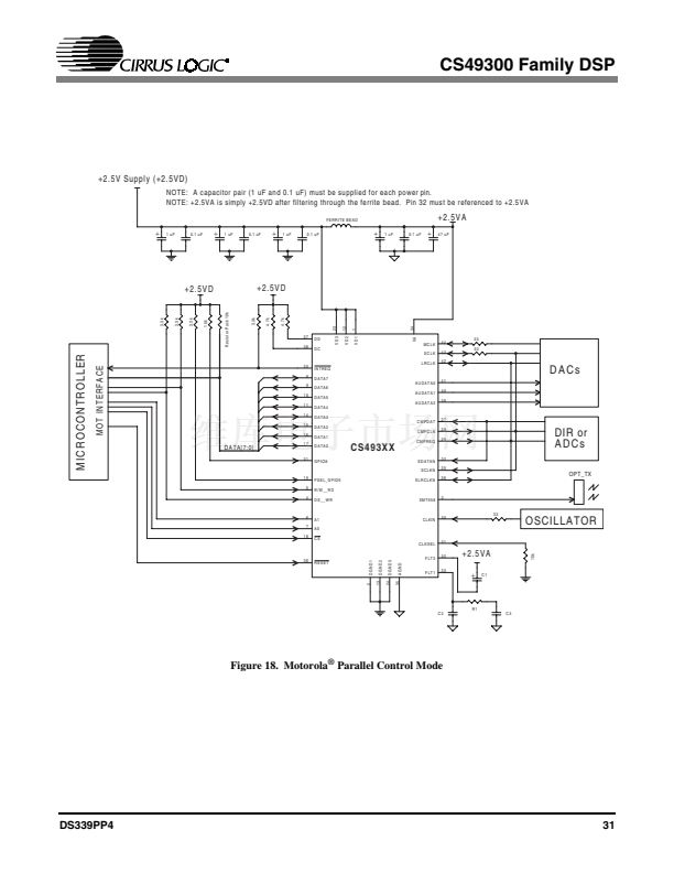
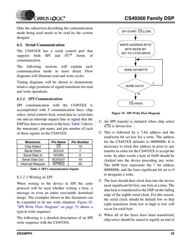
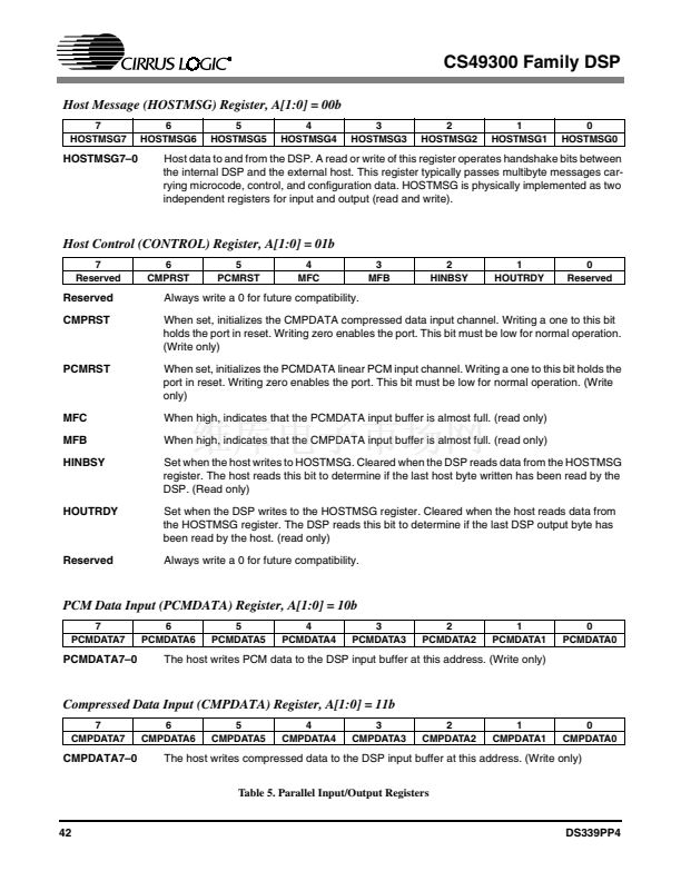
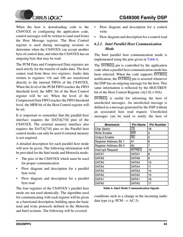
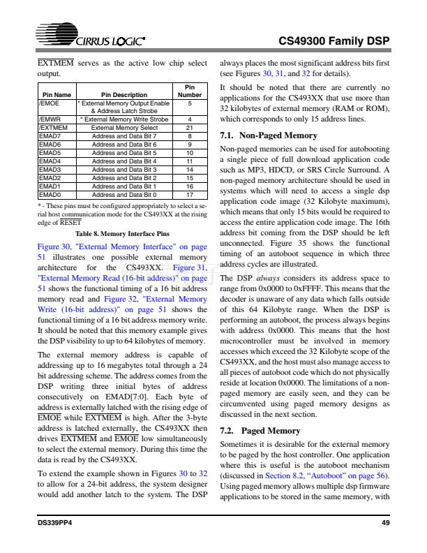
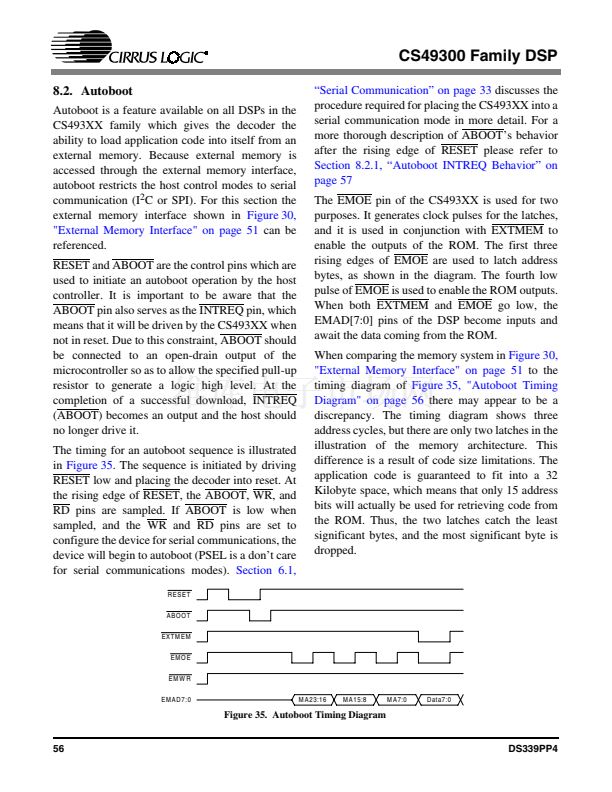
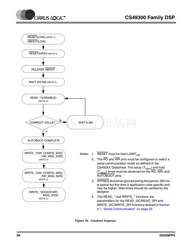
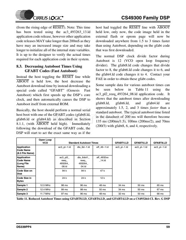
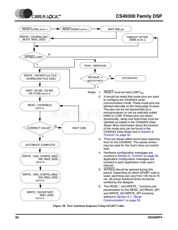
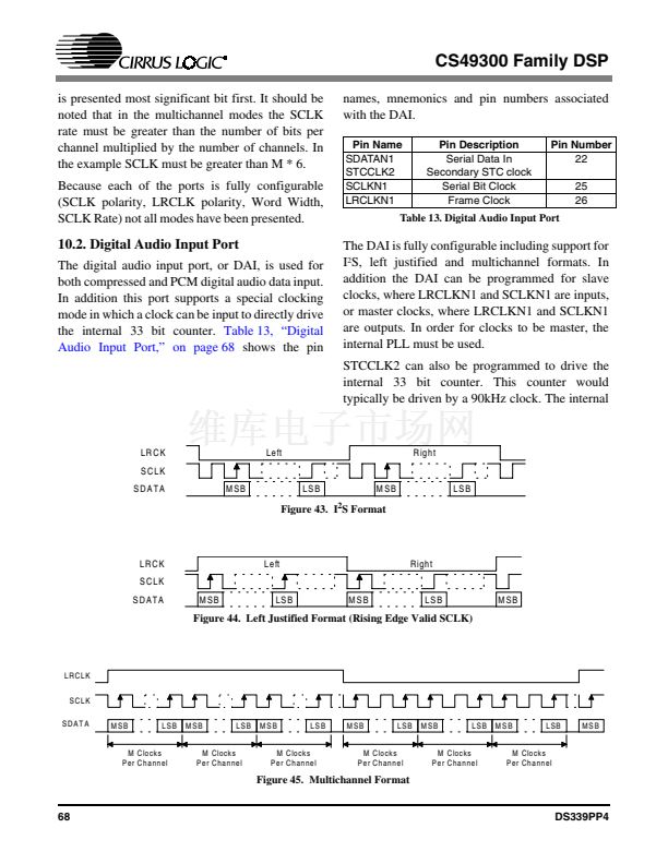
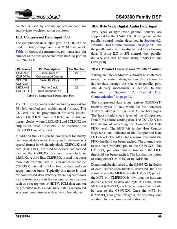
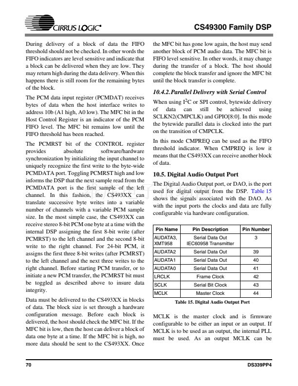
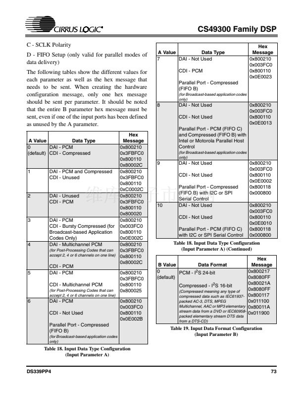
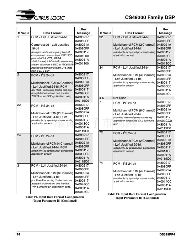
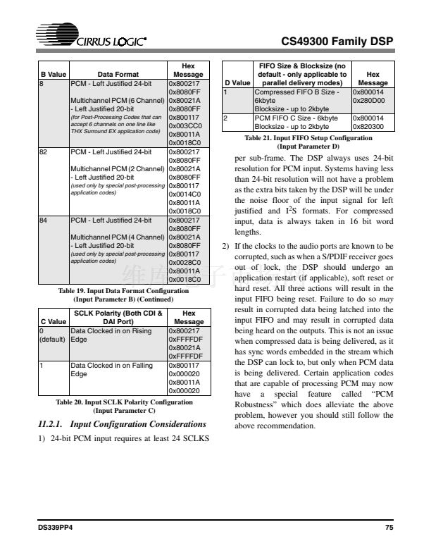
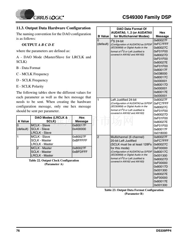
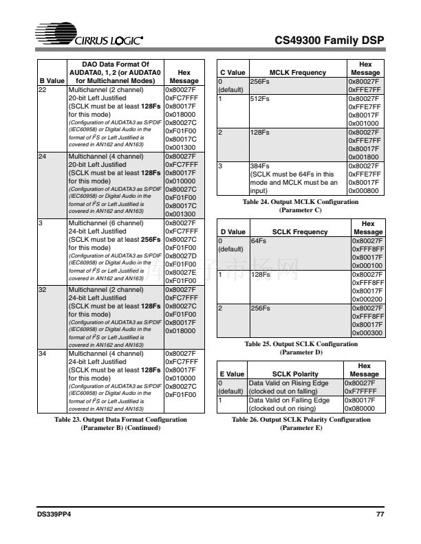
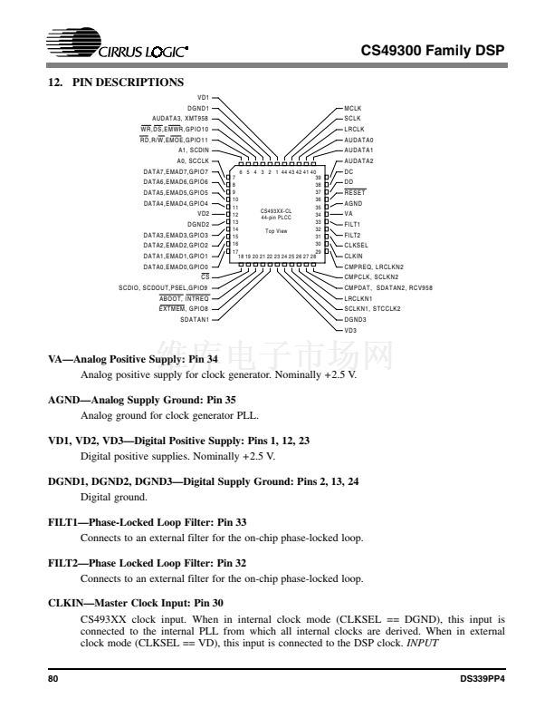
CS49300 Family DSP
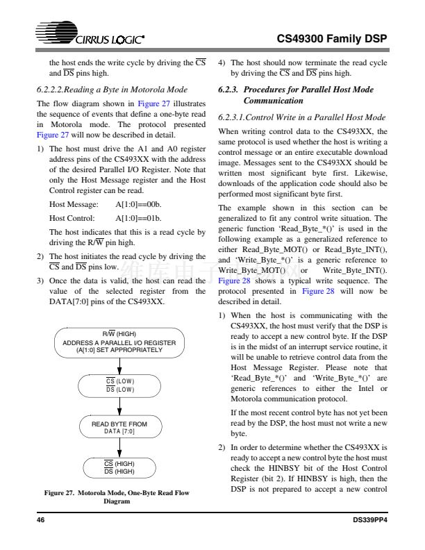
the host ends the write cycle by driving the CS
and DS pins high.
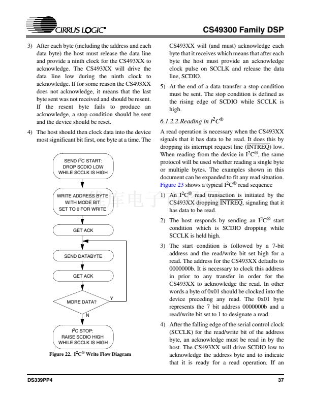
4) The host should now terminate the read cycle
by driving the CS and DS pins high.
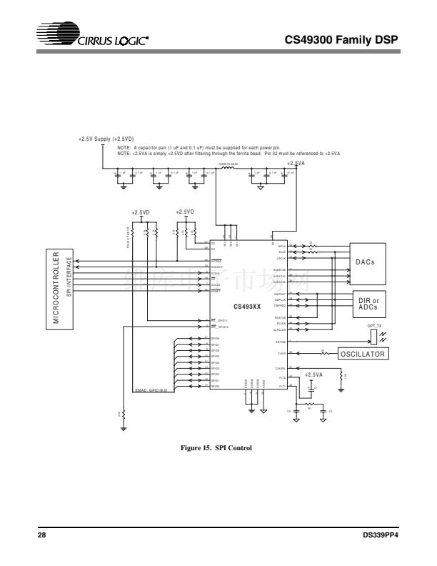
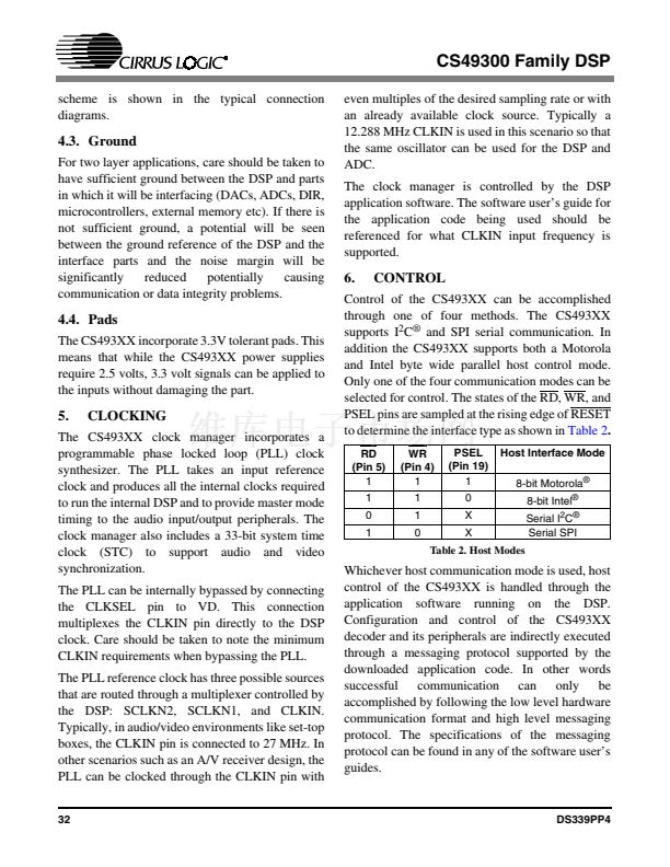
6.2.2.2.Reading a Byte in Motorola Mode
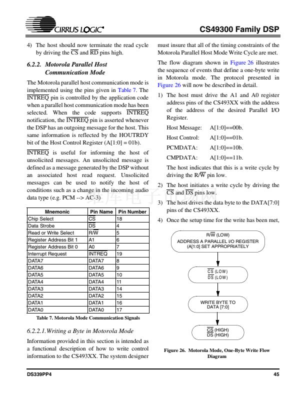
The flow diagram shown in
Figure 27
illustrates
the sequence of events that define a one-byte read
in Motorola mode. The protocol presented
Figure 27
will now be described in detail.
1) The host must drive the A1 and A0 register
address pins of the CS493XX with the address
of the desired Parallel I/O Register. Note that
only the Host Message register and the Host
Control register can be read.
Host Message:
Host Control:
A[1:0]==00b.
A[1:0]==01b.
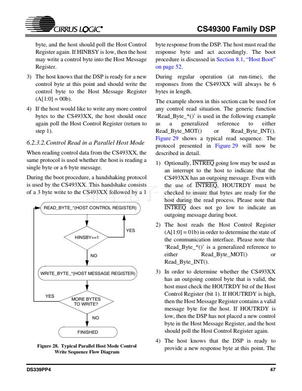
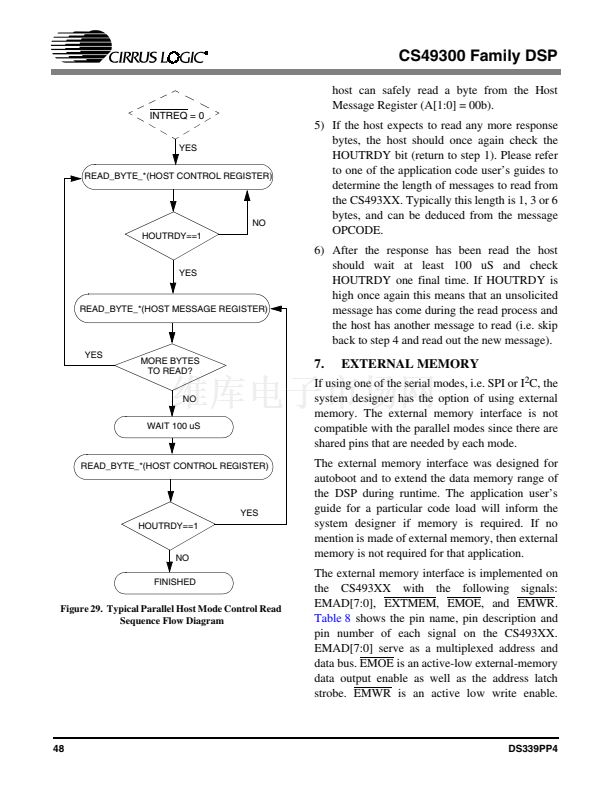
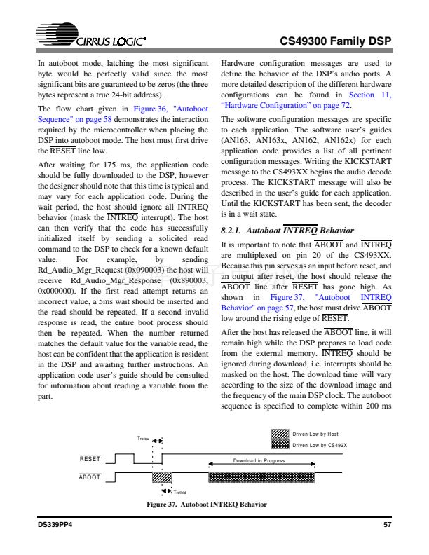
6.2.3. Procedures for Parallel Host Mode
Communication
6.2.3.1.Control Write in a Parallel Host Mode
When writing control data to the CS493XX, the
same protocol is used whether the host is writing a
control message or an entire executable download
image. Messages sent to the CS493XX should be
written most significant byte first. Likewise,
downloads of the application code should also be
performed most significant byte first.
The example shown in this section can be
generalized to fit any control write situation. The
generic function 鈥楻ead_Byte_*()鈥?is used in the
following example as a generalized reference to
either Read_Byte_MOT() or Read_Byte_INT(),
and 鈥榃rite_Byte_*()鈥?is a generic reference to
Write_Byte_MOT()
or
Write_Byte_INT().
Figure 28
shows a typical write sequence. The
protocol presented in
Figure 28
will now be
described in detail.
1) When the host is communicating with the
CS493XX, the host must verify that the DSP is
ready to accept a new control byte. If the DSP
is in the midst of an interrupt service routine, it
will be unable to retrieve control data from the
Host Message Register. Please note that
鈥楻ead_Byte_*()鈥?and 鈥榃rite_Byte_*()鈥?are
generic references to either the Intel or
Motorola communication protocol.
If the most recent control byte has not yet been
read by the DSP, the host must not write a new
byte.
2) In order to determine whether the CS493XX is
ready to accept a new control byte the host must
check the HINBSY bit of the Host Control
Register (bit 2). If HINBSY is high, then the
DSP is not prepared to accept a new control
The host indicates that this is a read cycle by
driving the R/W pin high.
2) The host initiates the read cycle by driving the
CS and DS pins low.
3) Once the data is valid, the host can read the
value of the selected register from the
DATA[7:0] pins of the CS493XX.
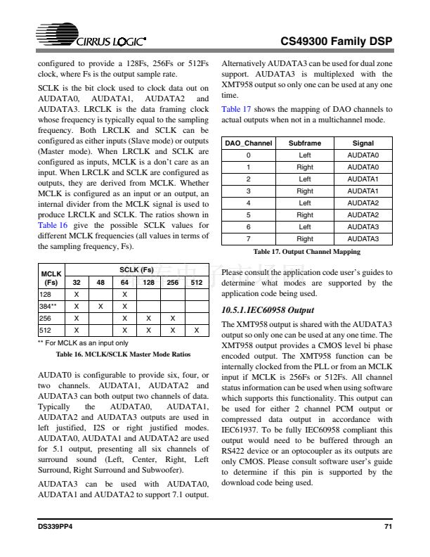
R/W (HIGH)
ADDRESS A PARALLEL I/O REGISTER
(A[1:0] SET APPROPRIATELY
C S (L O W )
D S (L O W )
READ BYTE FROM
D A TA [7:0]
CS (HIGH)
DS (HIGH)
Figure 27. Motorola Mode, One-Byte Read Flow
Diagram
46
DS339PP4


 1
1
 2
2
 3
3
 4
4
 5
5
 6
6
 7
7
 8
8
 9
9
 10
10
 11
11
 12
12
 13
13
 14
14
 15
15
 16
16
 17
17
 18
18
 19
19
 20
20
 21
21
 22
22
 23
23
 24
24
 25
25
 26
26
 27
27
 28
28
 29
29
 30
30
 31
31
 32
32
 33
33
 34
34
 35
35
 36
36
 37
37
 38
38
 39
39
 40
40
 41
41
 42
42
 43
43
 44
44
 45
45
 46
46
 47
47
 48
48
 49
49
 50
50
 51
51
 52
52
 53
53
 54
54
 55
55
 56
56
 57
57
 58
58
 59
59
 60
60
 61
61
 62
62
 63
63
 64
64
 65
65
 66
66
 67
67
 68
68
 69
69
 70
70
 71
71
 72
72
 73
73
 74
74
 75
75
 76
76
 77
77
 78
78
 79
79
 80
80
 81
81
 82
82
 83
83
 84
84
 85
85
 86
86
