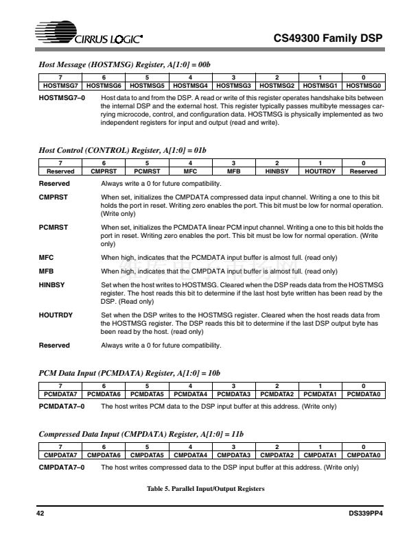
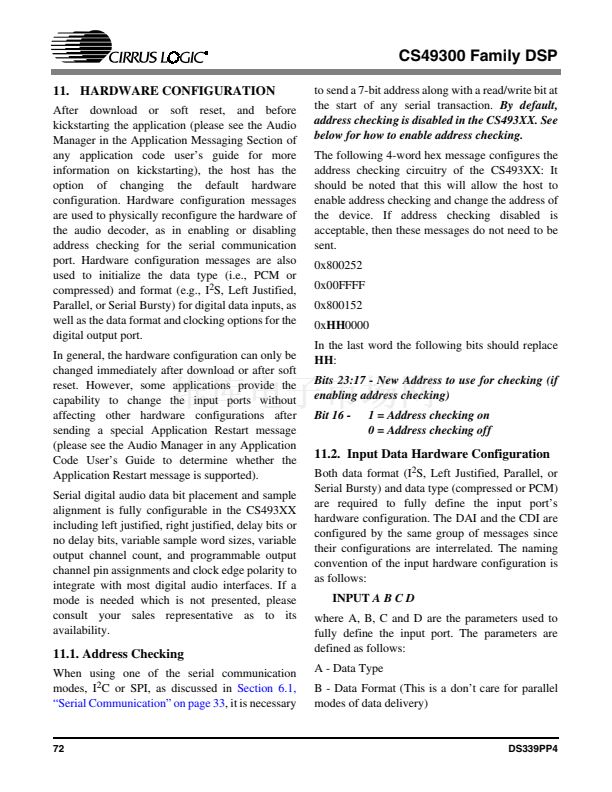
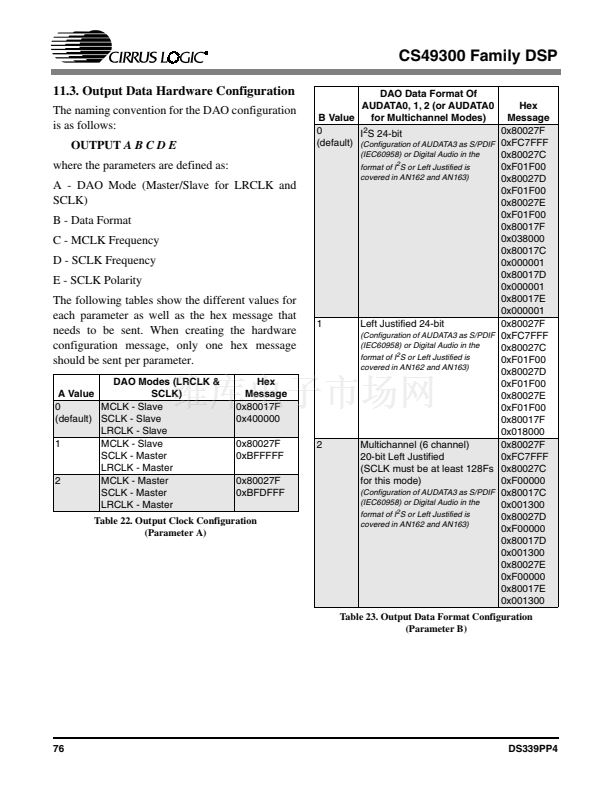
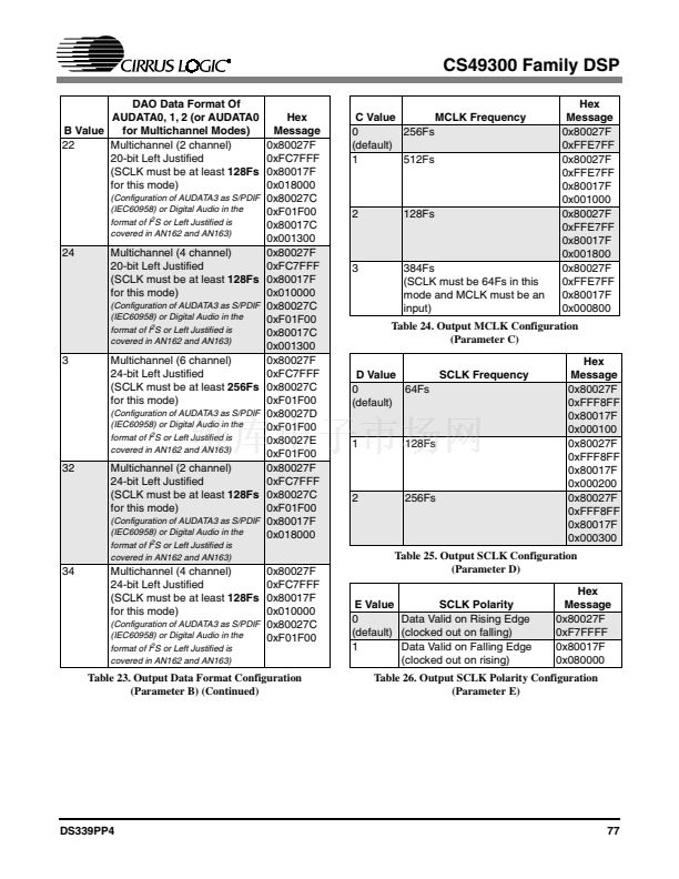
40
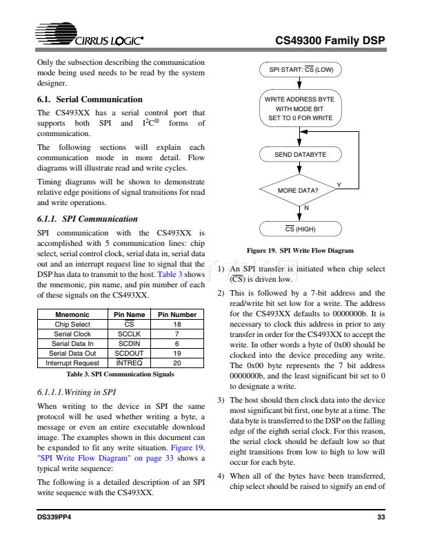
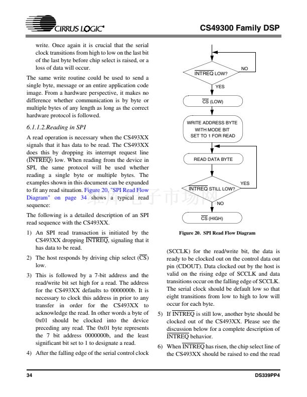
I
2
C Stop
D7
D6
D5
D4
D3
D2
D1
D0
AC K D 7
D6
D5
D4
D3
D2
D1
D0
AC K D7
D6
D5
D4
D3
D2
D1
D0
A CK
I
2
C Start
SCCLK
SCDIO
A D6 A D5 A D 4 A D3 A D 2 A D 1 A D 0 R/W A C K
I
2
C W rite Functional Tim ing
I
2
C Start
I
2
C Stop
SCCLK
AC K
D7
D6
D5
D4
D3
D2
D1
D0
ACK
D7
D6
D5
D4
D3
D2
D1
D0
ACK
D7
D6
D5
D4
D3
D2
D1
D0
NA CK
SCDIO
AD 6 AD 5
A D4 A D3 A D 2 A D1 A D0 R /W
INTREQ
Note 1
Note 2
Note 3
Note 4
Note 5
I
2
C Read Functional Tim ing
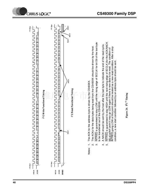
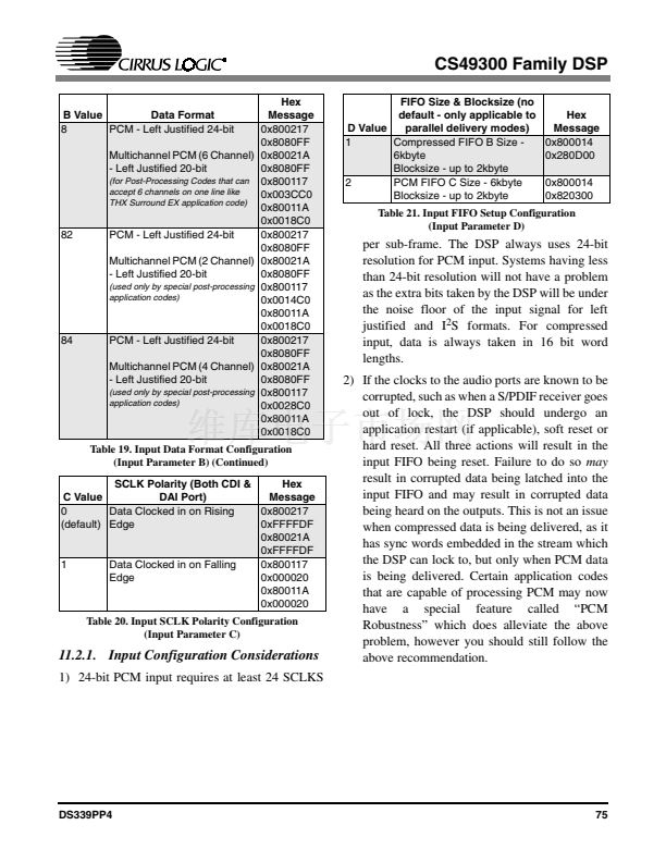
Notes: 1. The ACK for the address byte is driven by the CS493XX.
2. The ACKs for the data bytes being read from the CS493XX should be driven by the host.
3. INTREQ is guaranteed to stay LOW until the rising edge of SCCLK for bit D0 of the last byte
to be transferred out of the CS493XX.
4. A NACK should be sent by the host after the last byte to indicate the end of the read cycle.
5. INTREQ is guaranteed to stay HIGH until the next rising edge of SCCLK (for the ACK/NACK
bit) at which point it may go LOW again if there is new data to be read. The condition of
INTREQ going LOW at this point should be treated as a new read condition. After a stop
condition, a new start condition followed by an address byte should be sent.
CS49300 Family DSP
DS339PP4
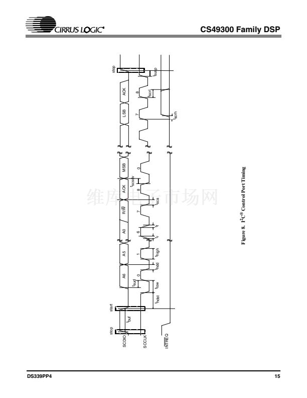
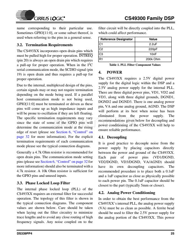
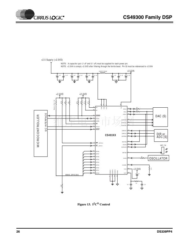
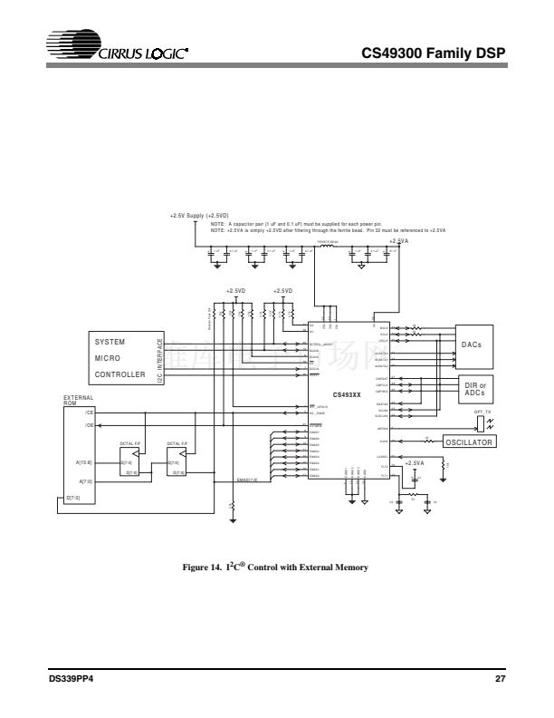
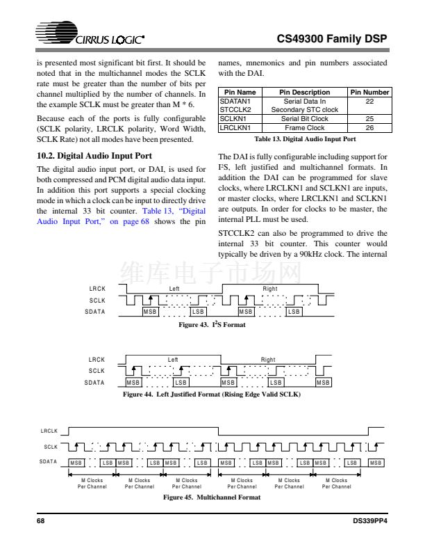
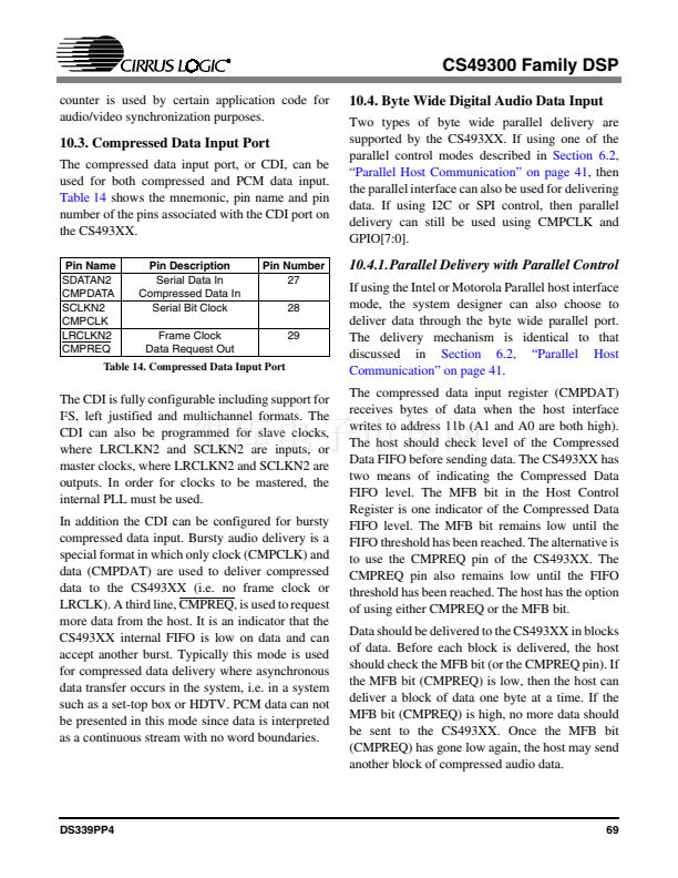
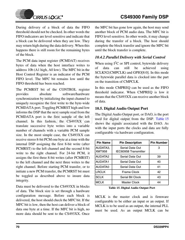
Figure 24. I
2
C
廬
Timing


 1
1
 2
2
 3
3
 4
4
 5
5
 6
6
 7
7
 8
8
 9
9
 10
10
 11
11
 12
12
 13
13
 14
14
 15
15
 16
16
 17
17
 18
18
 19
19
 20
20
 21
21
 22
22
 23
23
 24
24
 25
25
 26
26
 27
27
 28
28
 29
29
 30
30
 31
31
 32
32
 33
33
 34
34
 35
35
 36
36
 37
37
 38
38
 39
39
 40
40
 41
41
 42
42
 43
43
 44
44
 45
45
 46
46
 47
47
 48
48
 49
49
 50
50
 51
51
 52
52
 53
53
 54
54
 55
55
 56
56
 57
57
 58
58
 59
59
 60
60
 61
61
 62
62
 63
63
 64
64
 65
65
 66
66
 67
67
 68
68
 69
69
 70
70
 71
71
 72
72
 73
73
 74
74
 75
75
 76
76
 77
77
 78
78
 79
79
 80
80
 81
81
 82
82
 83
83
 84
84
 85
85
 86
86
