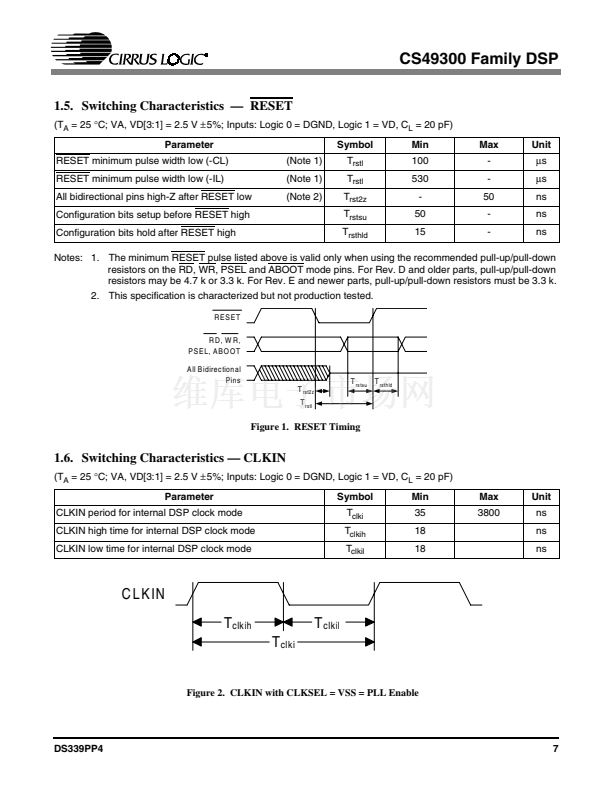
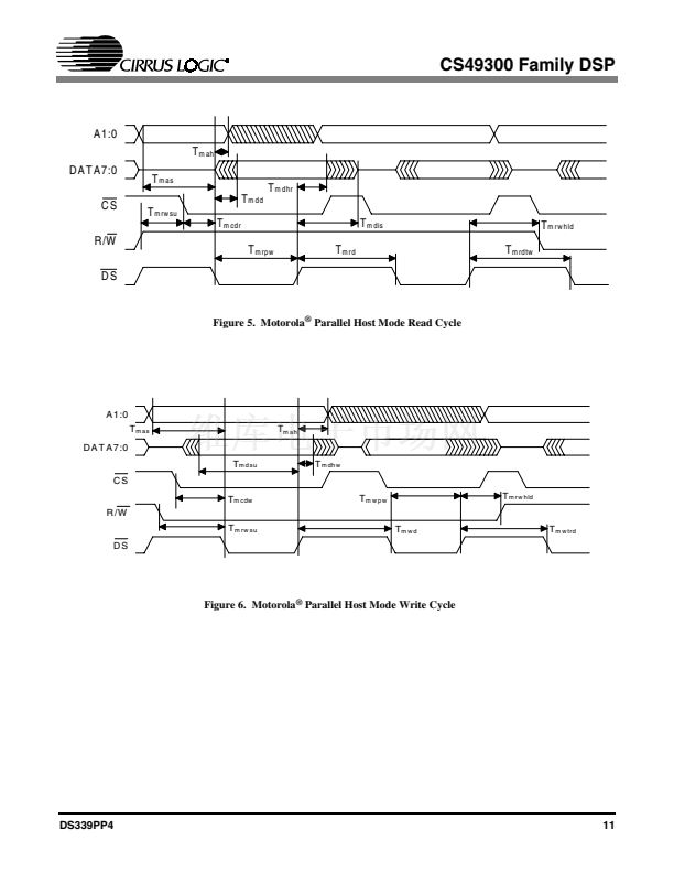
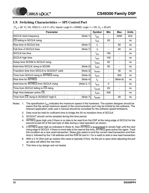
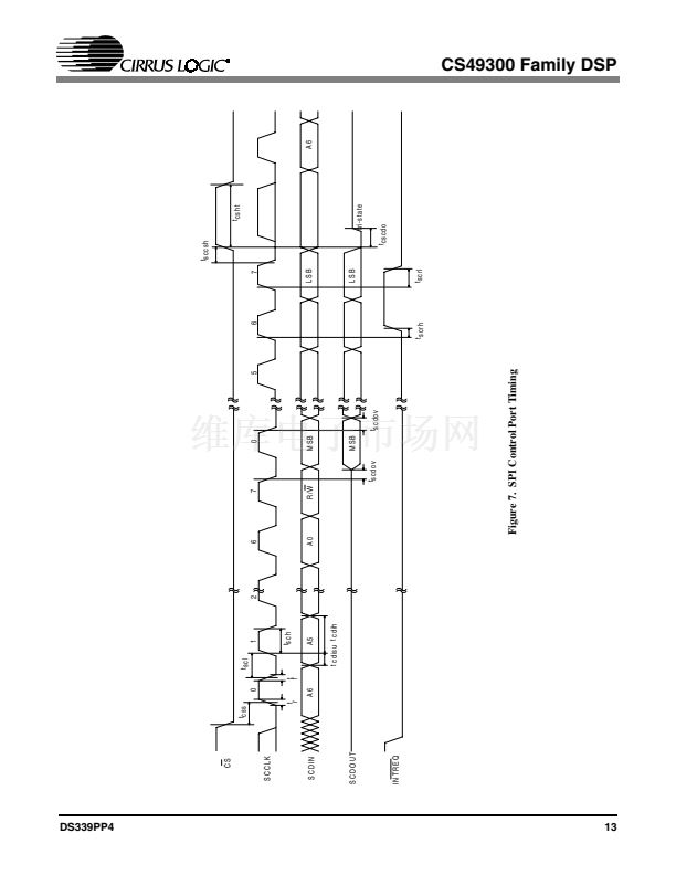
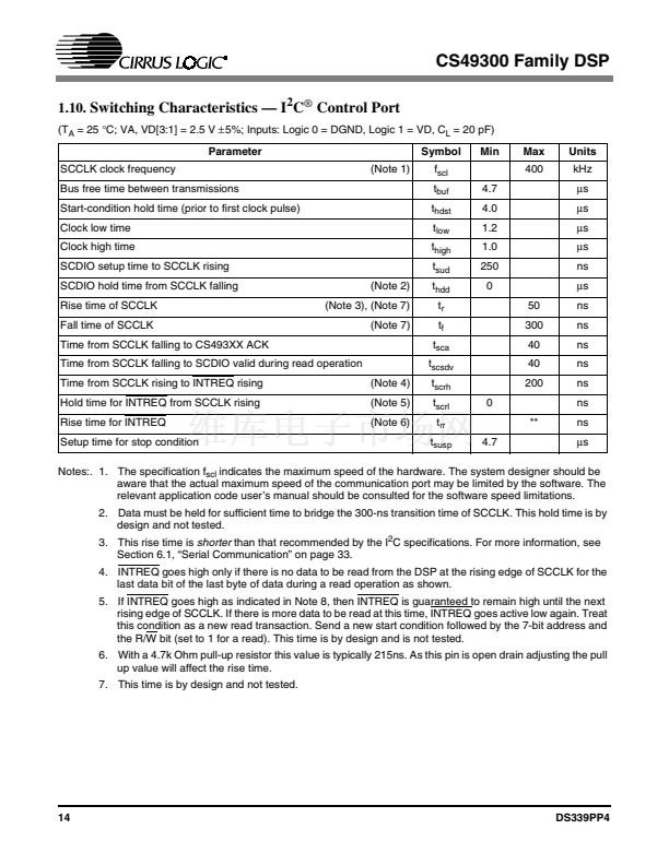
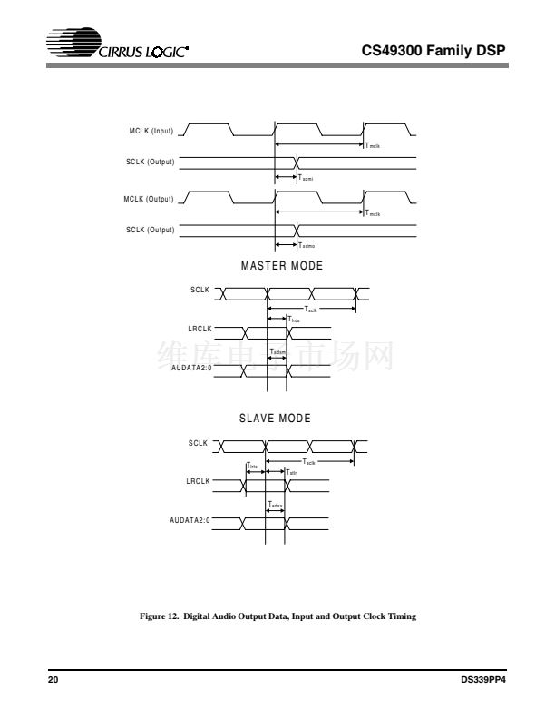
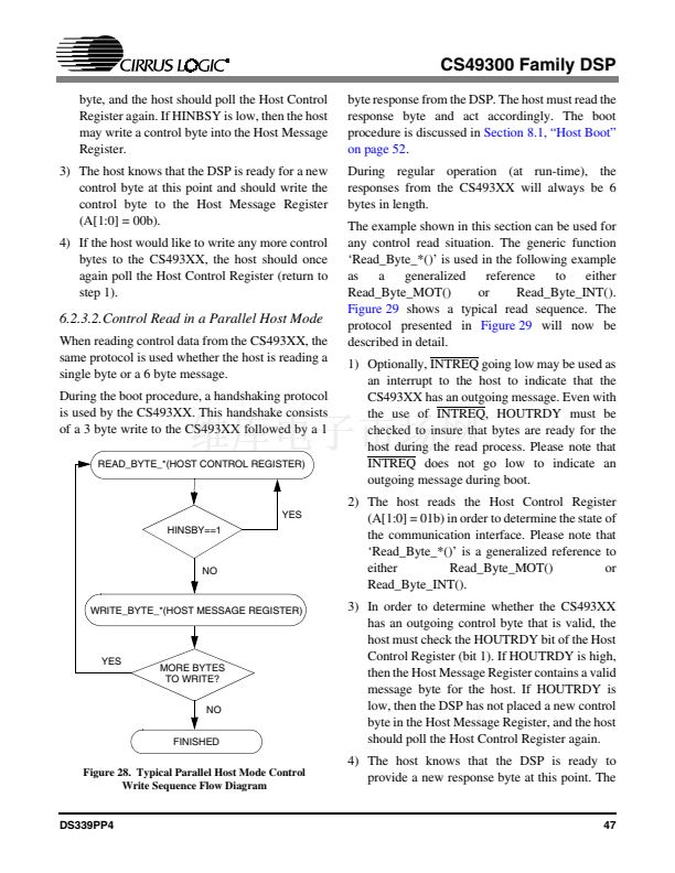
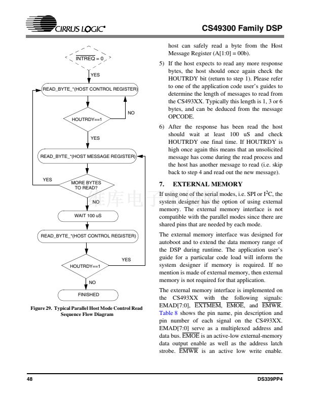
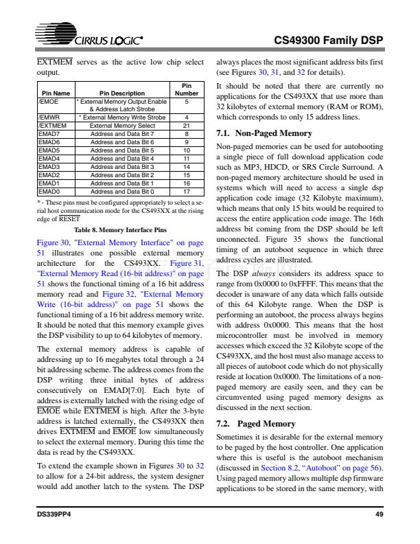
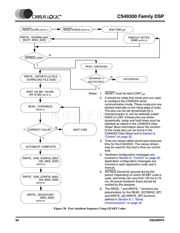
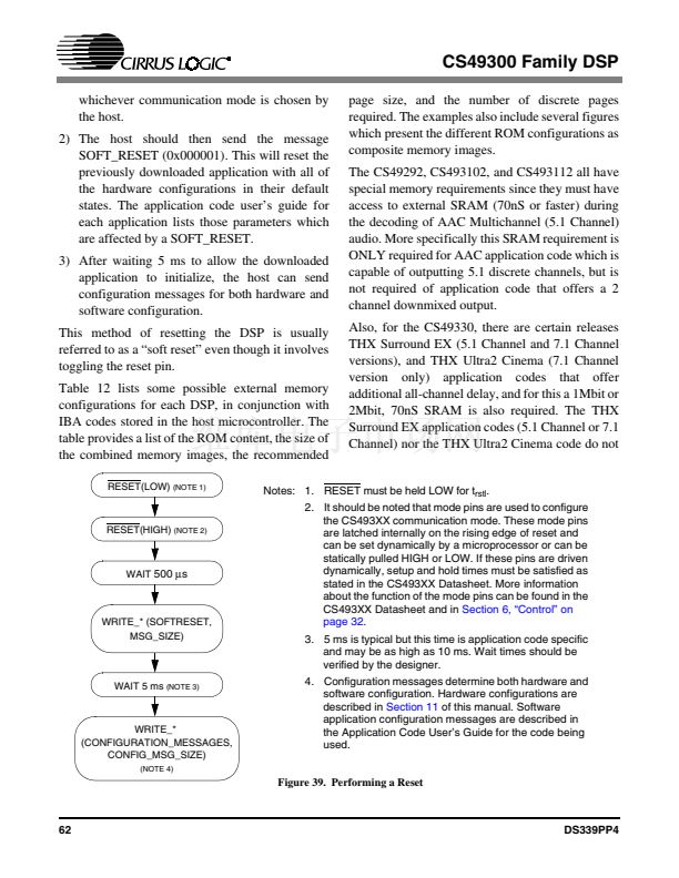
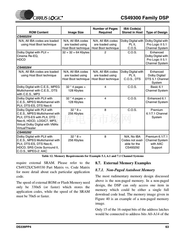
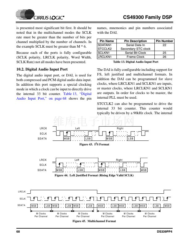
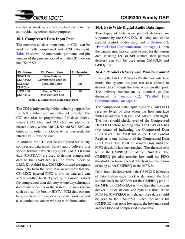
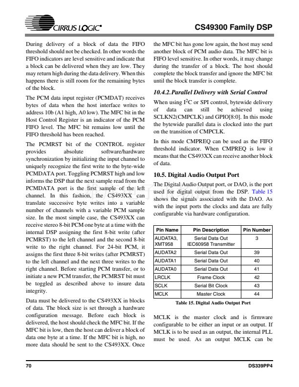
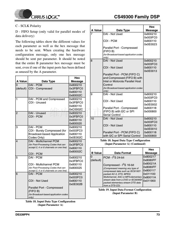
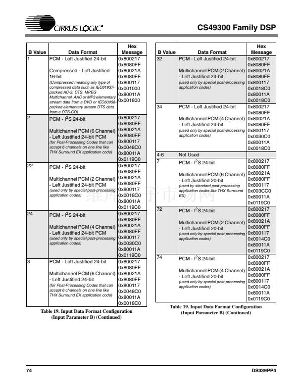
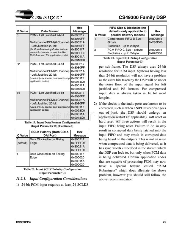
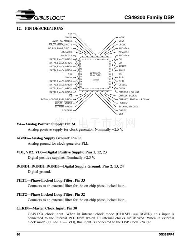
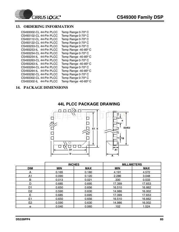
CS49300 Family DSP
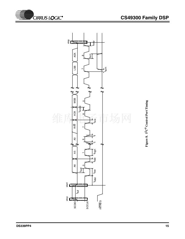
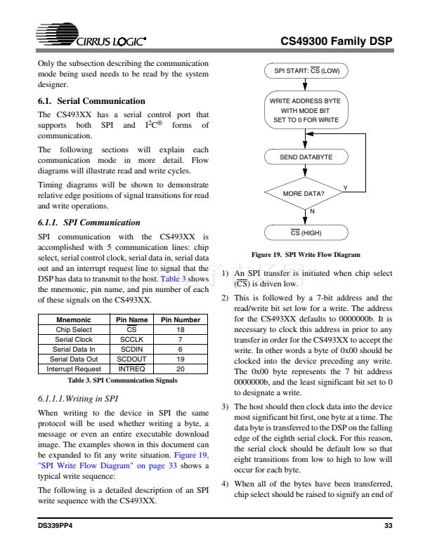
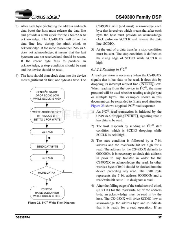
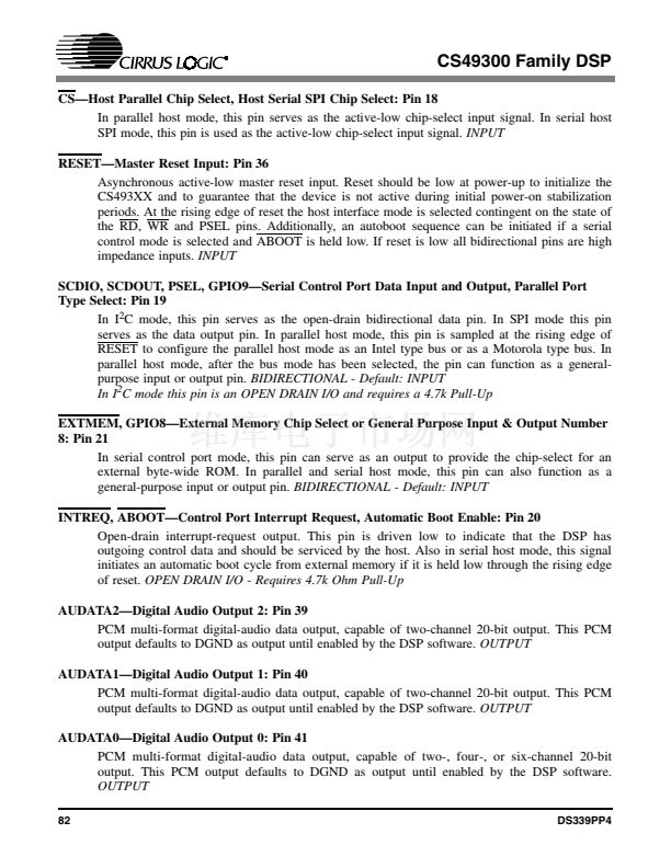
3) After each byte (including the address and each
data byte) the host must release the data line
and provide a ninth clock for the CS493XX to
acknowledge. The CS493XX will drive the
data line low during the ninth clock to
acknowledge. If for some reason the CS493XX
does not acknowledge, it means that the last
byte sent was not received and should be resent.
If the resent byte fails to produce an
acknowledge, a stop condition should be sent
and the device should be reset.
4) The host should then clock data into the device
most significant bit first, one byte at a time. The
SEND I
2
C START:
DROP SCDIO LOW
WHILE SCCLK IS HIGH
CS493XX will (and must) acknowledge each
byte that it receives which means that after each
byte the host must provide an acknowledge
clock pulse on SCCLK and release the data
line, SCDIO.
5) At the end of a data transfer a stop condition
must be sent. The stop condition is defined as
the rising edge of SCDIO while SCCLK is
high.
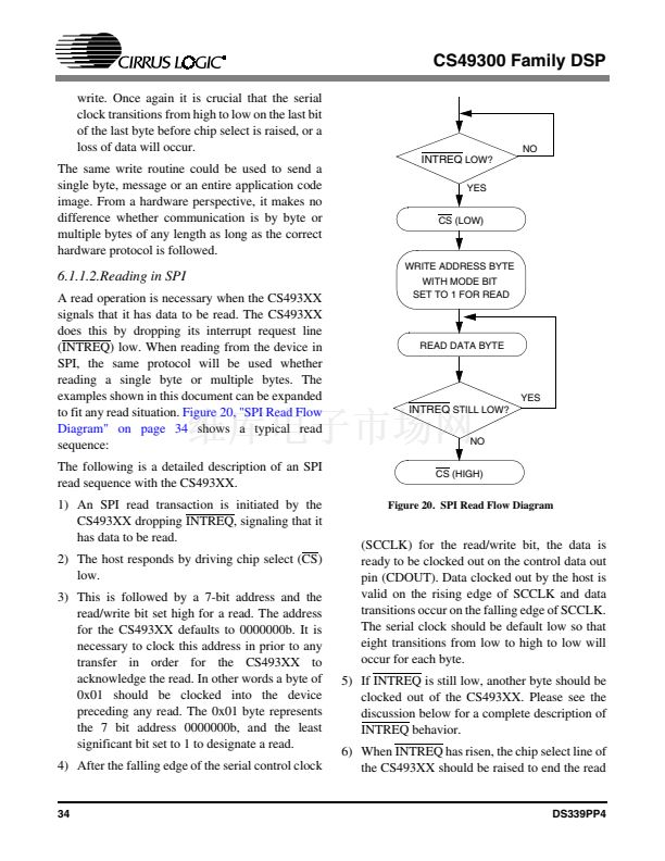
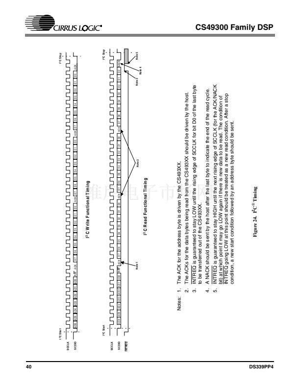
6.1.2.2.Reading in I
2
C
廬
A read operation is necessary when the CS493XX
signals that it has data to be read. It does this by
dropping its interrupt request line (INTREQ) low.
When reading from the device in I
2
C
廬
, the same
protocol will be used whether reading a single byte
or multiple bytes. The examples shown in this
document can be expanded to fit any read situation.
Figure 23
shows a typical I
2
C
廬
read sequence
1) An I
2
C
廬
read transaction is initiated by the
CS493XX dropping INTREQ, signaling that it
has data to be read.
2) The host responds by sending an I
2
C
廬
start
condition which is SCDIO dropping while
SCCLK is held high.
3) The start condition is followed by a 7-bit
address and the read/write bit set high for a
read. The address for the CS493XX defaults to
0000000b. It is necessary to clock this address
in prior to any transfer in order for the
CS493XX to acknowledge the read. In other
words a byte of 0x01 should be clocked into the
device preceding any read. The 0x01 byte
represents the 7 bit address 0000000b and a
read/write bit set to 1 to designate a read.
4) After the falling edge of the serial control clock
(SCCLK) for the read/write bit of the address
byte, an acknowledge must be read in by the
host. The CS493XX will drive SCDIO low to
acknowledge the address byte and to indicate
that it is ready for a read operation. If an
37
WRITE ADDRESS BYTE
WITH MODE BIT
SET TO 0 FOR WRITE
GET ACK
SEND DATABYTE
GET ACK
MORE DATA?
N
2
C
Y
I STOP:
RAISE SCDIO HIGH
WHILE SCCLK IS HIGH
Figure 22. I
2
C
廬
Write Flow Diagram
DS339PP4


 1
1
 2
2
 3
3
 4
4
 5
5
 6
6
 7
7
 8
8
 9
9
 10
10
 11
11
 12
12
 13
13
 14
14
 15
15
 16
16
 17
17
 18
18
 19
19
 20
20
 21
21
 22
22
 23
23
 24
24
 25
25
 26
26
 27
27
 28
28
 29
29
 30
30
 31
31
 32
32
 33
33
 34
34
 35
35
 36
36
 37
37
 38
38
 39
39
 40
40
 41
41
 42
42
 43
43
 44
44
 45
45
 46
46
 47
47
 48
48
 49
49
 50
50
 51
51
 52
52
 53
53
 54
54
 55
55
 56
56
 57
57
 58
58
 59
59
 60
60
 61
61
 62
62
 63
63
 64
64
 65
65
 66
66
 67
67
 68
68
 69
69
 70
70
 71
71
 72
72
 73
73
 74
74
 75
75
 76
76
 77
77
 78
78
 79
79
 80
80
 81
81
 82
82
 83
83
 84
84
 85
85
 86
86
