CS4923/4/5/6/7/8/9
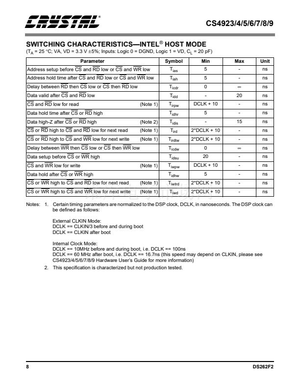
SWITCHING CHARACTERISTICS鈥擨NTEL
廬
HOST MODE
(T
A
= 25
擄C;
VA, VD = 3.3 V
鹵5%;
Inputs: Logic 0 = DGND, Logic 1 = VD, C
L
= 20 pF)
Parameter
Address setup before CS and RD low or CS and WR low
Address hold time after CS and RD low or CS and WR low
Delay between RD then CS low or CS then RD low
Data valid after CS and RD low
CS and RD low for read
Data hold time after CS or RD high
Data high-Z after CS or RD high
CS or RD high to CS and RD low for next read
CS or RD high to CS and WR low for next write
Delay between WR then CS low or CS then WR low
Data setup before CS or WR high
CS and WR low for write
Data hold after CS or WR high
CS or WR high to CS and RD low for next read
CS or WR high to CS and WR low for next write
(Note 1)
(Note 1)
(Note 1)
(Note 2)
(Note 1)
(Note 1)
(Note 1)
Symbol
T
ias
T
iah
T
icdr
T
idd
T
irpw
T
idhr
T
idis
T
ird
T
irdtw
T
icdw
T
idsu
T
iwpw
T
idhw
T
iwtrd
T
iwd
Min
5
5
0
-
DCLK + 10
5
-
2*DCLK + 10
2*DCLK + 10
0
20
DCLK + 10
5
2*DCLK + 10
2*DCLK + 10
Max
-
-
鈭?/div>
20
-
-
15
-
-
鈭?/div>
-
-
-
-
-
Unit
ns
ns
ns
ns
ns
ns
ns
ns
ns
ns
ns
ns
ns
ns
ns
Notes: 1. Certain timing parameters are normalized to the DSP clock, DCLK, in nanoseconds. The DSP clock can
be defined as follows:
External CLKIN Mode:
DCLK == CLKIN/3 before and during boot
DCLK == CLKIN after boot
Internal Clock Mode:
DCLK == 10MHz before and during boot, i.e. DCLK == 100ns
DCLK == 60 MHz after boot, i.e. DCLK == 16.7ns (this speed may depend on CLKIN, please see
CS4923/4/5/6/7/8/9 Hardware User鈥檚 Guide for more information)
2. This specification is characterized but not production tested.
8
DS262F2


 1
1
 2
2
 3
3
 4
4
 5
5
 6
6
 7
7
 8
8
 9
9
 10
10
 11
11
 12
12
 13
13
 14
14
 15
15
 16
16
 17
17
 18
18
 19
19
 20
20
 21
21
 22
22
 23
23
 24
24
 25
25
 26
26
 27
27
 28
28
 29
29
 30
30
 31
31
 32
32
 33
33
 34
34
 35
35
 36
36
 37
37
 38
38
 39
39
 40
40
 41
41
 42
42
 43
43
 44
44
 45
45
 46
46
 47
47
 48
48
 49
49
 50
50
 51
51
 52
52
 53
53
 54
54
 55
55
 56
56
