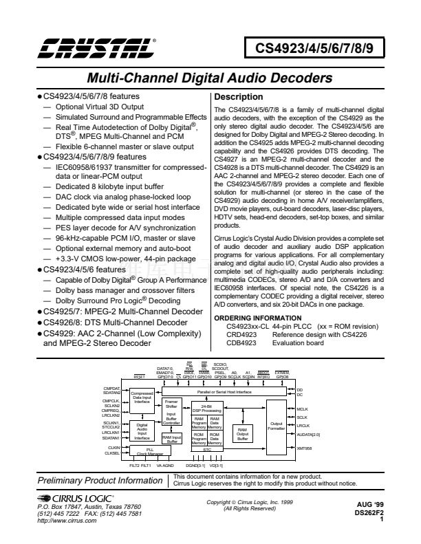
CS4923/4/5/6/7/8/9
covered in the CS4923/4/5/6/7/8/9 Hardware
User鈥檚 Guide. Application configuration is
described in the application code user鈥檚 guide for
the code being used.
each signal on the CS4923/4/5/6/7/8/9. RD and
WR have no effect when CS is held high.
When the DSP writes a byte to the HOSTMSG
register, the HOUTRDY bit in the CONTROL
register is set to indicate that there is data to be
read. To initiate a read cycle the host should drive
CS low. When CS is low, RD becomes the output
enable for DATA[7:0]. When CS and RD are low,
the contents of register address A[1:0] are driven
on the DATA[7:0] bus. The address A[1:0] must be
valid a minimum time before either CS or RD goes
low. The HOUTRDY bit of the CONTROL
register is cleared after the host reads from the
HOSTMSG register.
Driving both CS and WR low begins an 8-bit write
cycle. The address A[1:0] must be valid a
minimum time before either CS or WR goes low.
On the first rising edge of CS or WR, the write
cycle ends and DATA[7:0] are latched internally
by the CS492X. Data must be held sufficiently to
satisfy the hold time as given in the timing section.
The HINBSY bit is set when the host writes the
HOSTMSG register. This bit is cleared when the
byte in the HOSTMSG register is read by the DSP.
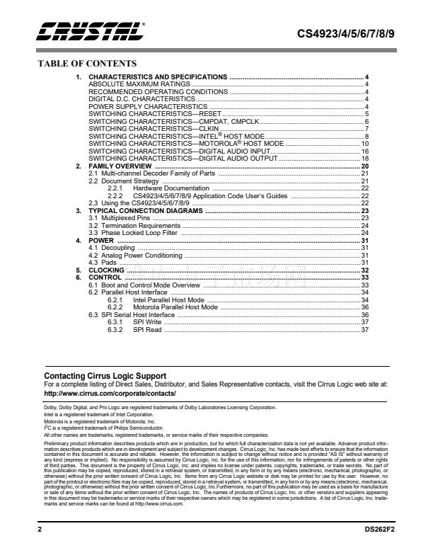
During RESET low, all control signals have no
effect and DATA[7:0] are high impedance.
Pin Name
CS
RD
WR
A1
A0
INTREQ
DATA7
DATA6
DATA5
DATA4
DATA3
DATA2
DATA1
DATA0
Pin Description
Chip Select
Output Enable
Write Enable
Register Address 1
Register Address 0
Interrupt Request
Data Bit 7
Data Bit 6
Data Bit 5
Data Bit 4
Data Bit 3
Data Bit 2
Data Bit 1
Data Bit 0
Pin Number
18
5
4
6
7
20
8
9
10
11
14
15
16
17
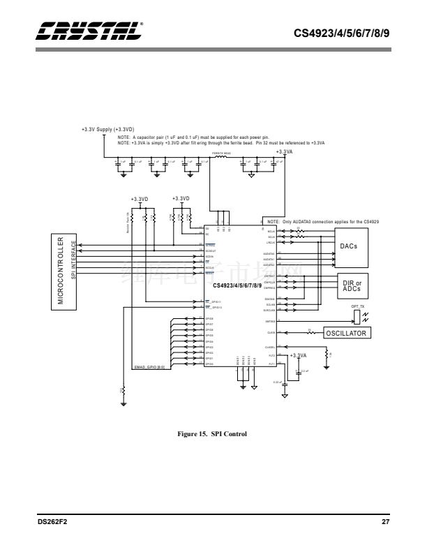
6.2 Parallel Host Interface
The byte wide parallel host interface of the
CS492X supports application code download,
communication for hardware and application
configuration, compressed data input, and PCM
data input. When using either Intel or Motorola
modes, the parallel interface is implemented using
four 8-bit internal registers which are selectable
using inputs A1 and A0 as shown in table 3. Table
5 shows the individual registers and their bit
mapping.
In either the Intel or Motorola mode the INTREQ
pin can be used to interrupt the host when the DSP
has unsolicited outgoing messages to be read. For
specific details on the behavior of INTREQ in one
of the parallel modes, please see the
CS4923/4/5/6/7/8/9 Hardware User鈥檚 Guide.
A1
A0 Register Name Register Function
(Pin 6) (Pin 7)
1
1
CMPDATA
8-bit compressed
data to input unit
(write only)
1
0
PCMDATA
8-bit linear PCM data
to input unit (write
only)
0
1
CONTROL Multi-bit control regis-
ter for setup and
handshaking (R/W)
0
0
HOSTMSG 8-bit control pipe
message register
(R/W)
Table 3. Host Memory Map
6.2.1 Intel Parallel Host Mode
Intel parallel host mode is accomplished with CS,
RD, WR, A[1:0], and DATA[7:0]. Table 4 shows
the pin name, pin description and pin number of
Table 4. Intel Parallel Host Mode Pin Assignments
34
DS262F2


 1
1
 2
2
 3
3
 4
4
 5
5
 6
6
 7
7
 8
8
 9
9
 10
10
 11
11
 12
12
 13
13
 14
14
 15
15
 16
16
 17
17
 18
18
 19
19
 20
20
 21
21
 22
22
 23
23
 24
24
 25
25
 26
26
 27
27
 28
28
 29
29
 30
30
 31
31
 32
32
 33
33
 34
34
 35
35
 36
36
 37
37
 38
38
 39
39
 40
40
 41
41
 42
42
 43
43
 44
44
 45
45
 46
46
 47
47
 48
48
 49
49
 50
50
 51
51
 52
52
 53
53
 54
54
 55
55
 56
56
