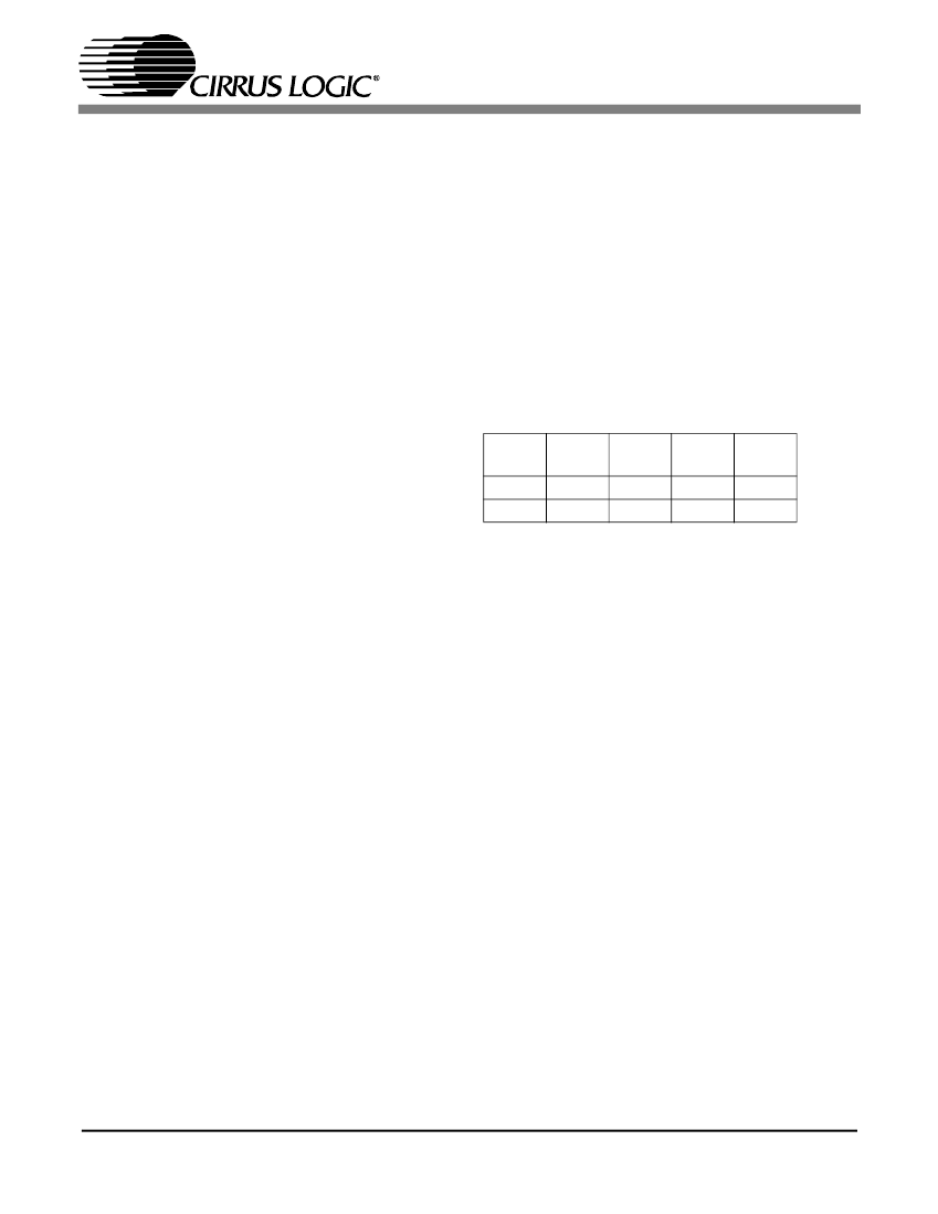
3 K鈩?/div>
Cflt
220 nF
22 nF
Crip
10 nF
1 nF
Settling
Time
11ms
4ms
medium
fast
Table 2. External PLL Component Values
5.2.1
OMCK System Clock Mode
A special clock switching mode is available that al-
lows the OMCK clock input to replace RMCK
when the PLL becomes unlocked.
In Software mode this feature is enabled by setting
SWCLK bit in Control1 register to a 鈥?鈥?
In Hardware Mode this feature is always active.
Clock switching is accomplished without spurious
transitions or glitches on RMCK.
OSCLK and OLRCK are derived from the OMCK
input when the clock has been switched and the se-
rial port is in master mode.
When the PLL loses lock, the frequency of the
VCO drops to ~500 kHz. When this system clock
mode is not enabled, the OSCLK and OLRCK will
be based on the VCO when the PLL is not locked
It is important to treat the PLL FLT pin as a low
level analog input. It is suggested that the ground
end of the PLL filter be returned directly to the
AGND pin independently of the digital ground
plane.
5.3
Error Reporting and Hold Function
Software Mode
While decoding the incoming AES3 data stream,
the CS8416 can identify several kinds of error, in-
dicated in the Receiver Error register (0Ch).
The errors indicated are:
1) QCRC 鈥?CRC error in Q subcode data
2) CCRC 鈥?CRC error in channel status data
3) UNLOCK 鈥?PLL is not locked to incoming data
stream
4) V 鈥?Data Validity bit is set
5) CONF 鈥?Input data stream is near error condi-
tion due to jitter degradation
6) BIP 鈥?Biphase encoding error
7) PAR 鈥?Parity error in incoming data
17
5.2.2
PLL External Components
The PLL behavior is affected by the external filter
component values.
Figure 5
and
Figure 6
show the
DS578PP2


 1
1
 2
2
 3
3
 4
4
 5
5
 6
6
 7
7
 8
8
 9
9
 10
10
 11
11
 12
12
 13
13
 14
14
 15
15
 16
16
 17
17
 18
18
 19
19
 20
20
 21
21
 22
22
 23
23
 24
24
 25
25
 26
26
 27
27
 28
28
 29
29
 30
30
 31
31
 32
32
 33
33
 34
34
 35
35
 36
36
 37
37
 38
38
 39
39
 40
40
 41
41
 42
42
 43
43
 44
44
 45
45
 46
46
 47
47
 48
48
