47K鈩?/div>
CS8416
RMCK
OMCK
Clock Control
Clock Source
External
Interface
Hardware
Control
TXSEL1
NV/RERR
*
*
96KHZ
*
RCBL
*
U
*
C
*
AUDIO
AGND
FILT
TX
DGND
Rflt
Cflt
Crip
****
*
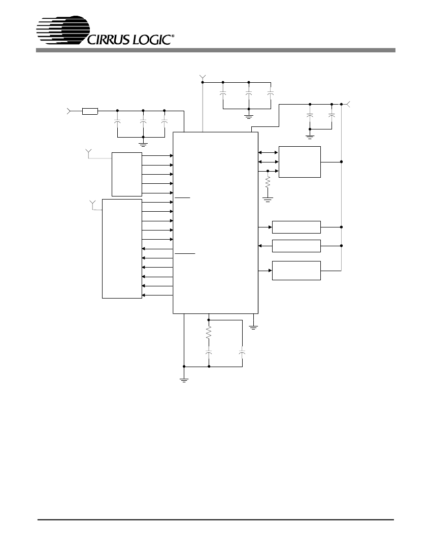
These pins must be pulled high to VL+ or low to DGND through a 47K鈩?resistor.
**
A seperate analog supply is only necessary in applications where RMCK is used for a jitter
sensitive tast. For applications where RMCK is not used for a jitter sensitive task, connect
VA+ to VD+ via a ferrite bead. Keep decoupling capacitors between VA+ and AGND.
***
Please see section 5.1 "8:2 S/PDIF Input Multiplexer" and Appendix
A for typical input configurations and recommended input circuits.
For best jitter performance connect the filter ground directly to the AGND pin.
****
See Table 2 for PLL filter values.
Figure 6. Typical Connection Diagram - Hardware Mode
DS578PP2
11


 1
1
 2
2
 3
3
 4
4
 5
5
 6
6
 7
7
 8
8
 9
9
 10
10
 11
11
 12
12
 13
13
 14
14
 15
15
 16
16
 17
17
 18
18
 19
19
 20
20
 21
21
 22
22
 23
23
 24
24
 25
25
 26
26
 27
27
 28
28
 29
29
 30
30
 31
31
 32
32
 33
33
 34
34
 35
35
 36
36
 37
37
 38
38
 39
39
 40
40
 41
41
 42
42
 43
43
 44
44
 45
45
 46
46
 47
47
 48
48
