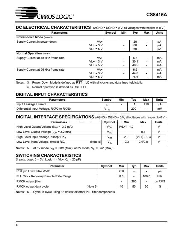
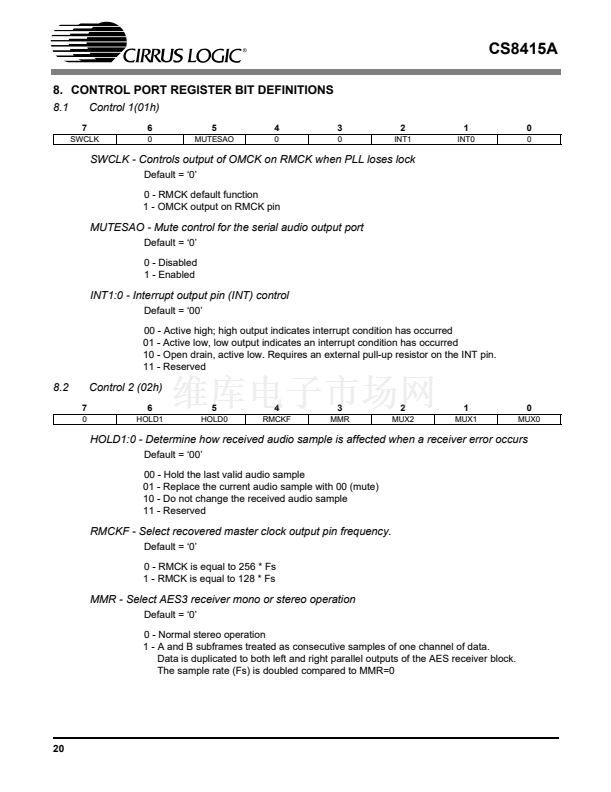
CS8415A
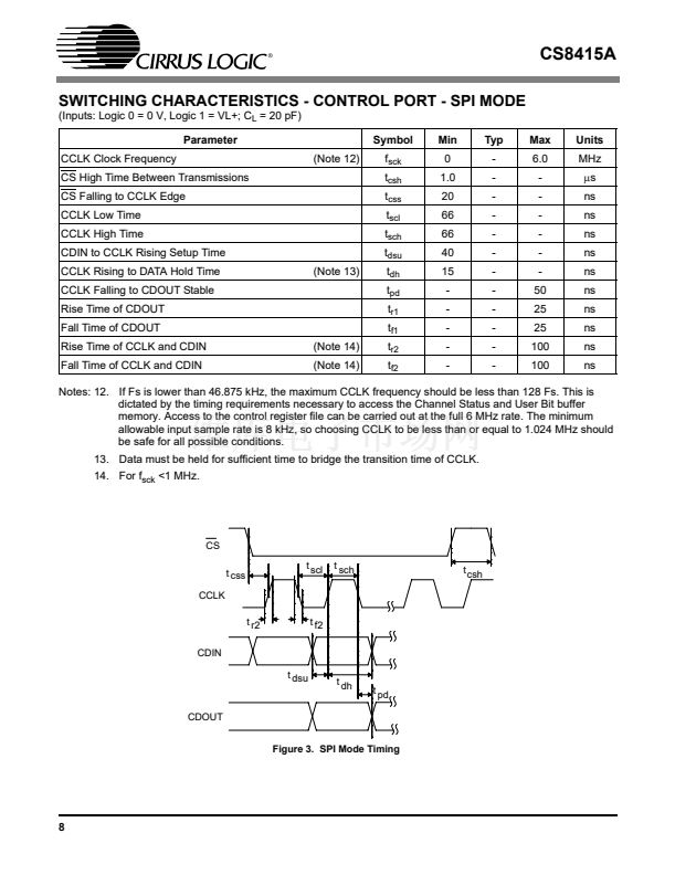
SWITCHING CHARACTERISTICS - CONTROL PORT - SPI MODE
(Inputs: Logic 0 = 0 V, Logic 1 = VL+; C
L
= 20 pF)
Parameter
CCLK Clock Frequency
CS High Time Between Transmissions
CS Falling to CCLK Edge
CCLK Low Time
CCLK High Time
CDIN to CCLK Rising Setup Time
CCLK Rising to DATA Hold Time
CCLK Falling to CDOUT Stable
Rise Time of CDOUT
Fall Time of CDOUT
Rise Time of CCLK and CDIN
Fall Time of CCLK and CDIN
(Note 14)
(Note 14)
(Note 13)
(Note 12)
Symbol
f
sck
t
csh
t
css
t
scl
t
sch
t
dsu
t
dh
t
pd
t
r1
t
f1
t
r2
t
f2
Min
0
1.0
20
66
66
40
15
-
-
-
-
-
Typ
-
-
-
-
-
-
-
-
-
-
-
-
Max
6.0
-
-
-
-
-
-
50
25
25
100
100
Units
MHz
碌s
ns
ns
ns
ns
ns
ns
ns
ns
ns
ns
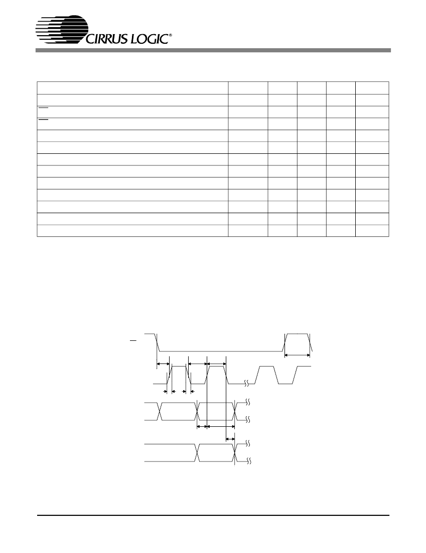
Notes: 12. If Fs is lower than 46.875 kHz, the maximum CCLK frequency should be less than 128 Fs. This is
dictated by the timing requirements necessary to access the Channel Status and User Bit buffer
memory. Access to the control register file can be carried out at the full 6 MHz rate. The minimum
allowable input sample rate is 8 kHz, so choosing CCLK to be less than or equal to 1.024 MHz should
be safe for all possible conditions.
13. Data must be held for sufficient time to bridge the transition time of CCLK.
14. For f
sck
<1 MHz.
CS
t css
CCLK
t r2
CDIN
t dsu
t dh
t f2
t scl
t sch
t csh
t pd
CDOUT
Figure 3. SPI Mode Timing
8


 1
1
 2
2
 3
3
 4
4
 5
5
 6
6
 7
7
 8
8
 9
9
 10
10
 11
11
 12
12
 13
13
 14
14
 15
15
 16
16
 17
17
 18
18
 19
19
 20
20
 21
21
 22
22
 23
23
 24
24
 25
25
 26
26
 27
27
 28
28
 29
29
 30
30
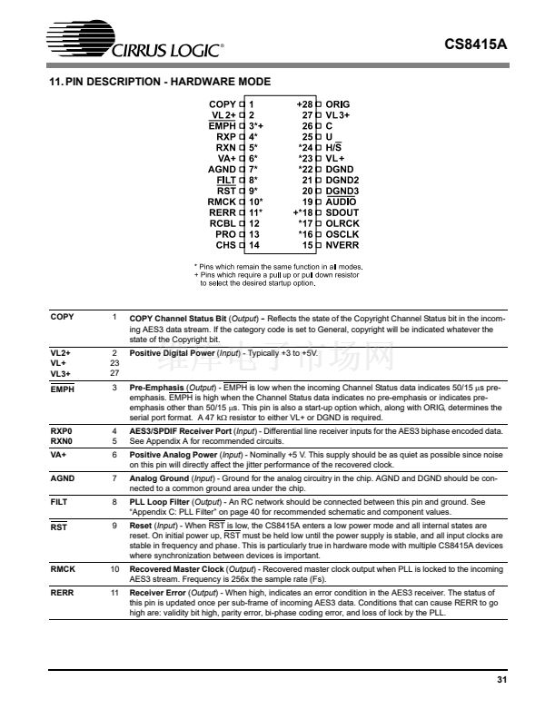 31
31
 32
32
 33
33
 34
34
 35
35
 36
36
 37
37
 38
38
 39
39
 40
40
 41
41
 42
42
