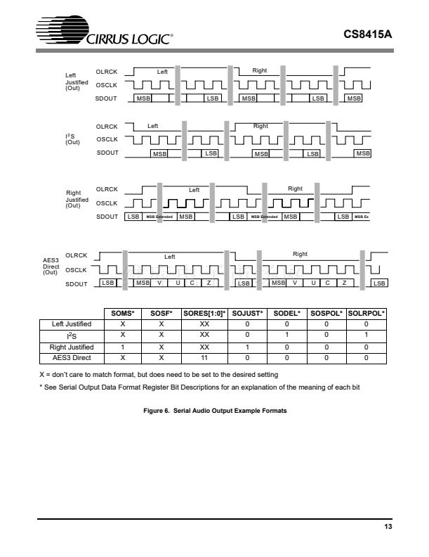
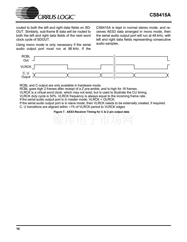
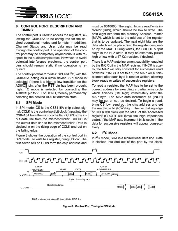
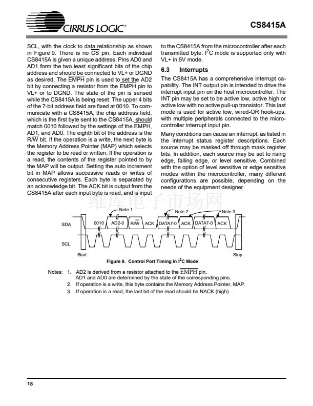
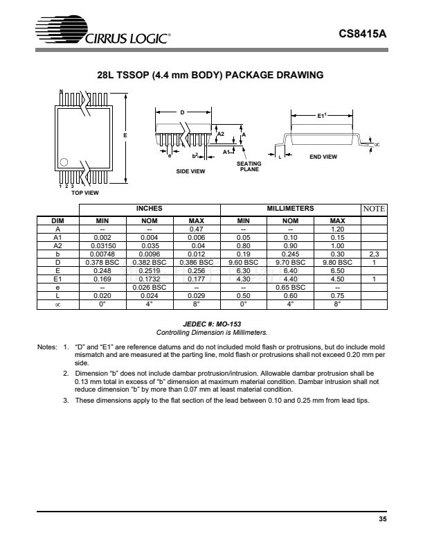
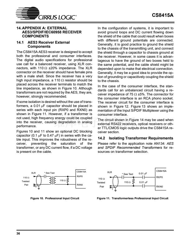
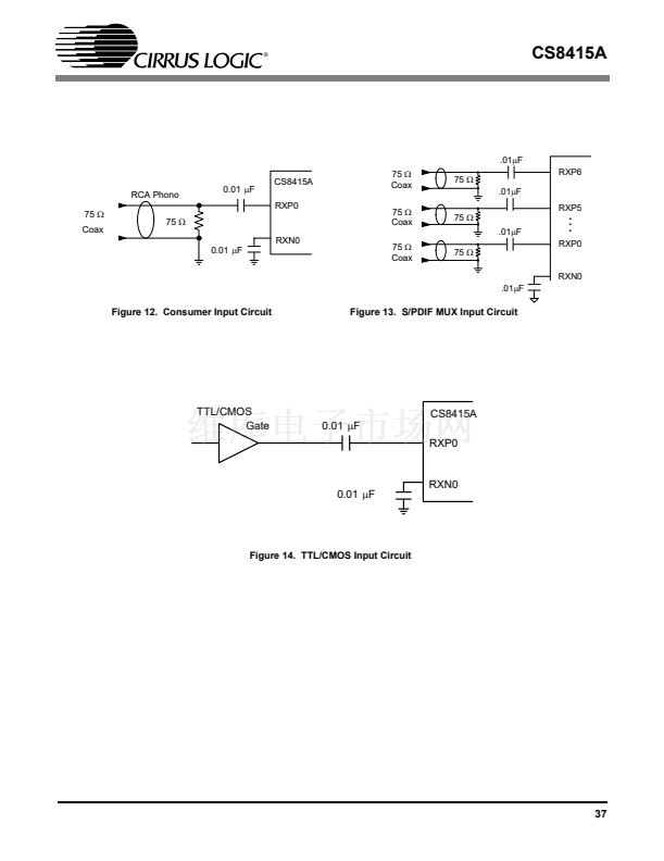
CS8415A
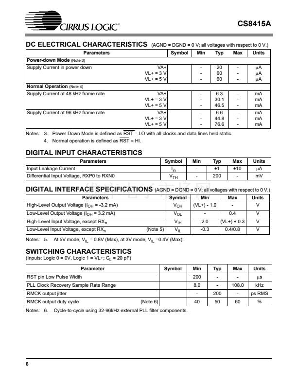
DC ELECTRICAL CHARACTERISTICS
Parameters
Power-down Mode
(Note 3)
Supply Current in power down
VA+
VL+ = 3 V
VL+ = 5 V
VA+
VL+ = 3 V
VL+ = 5 V
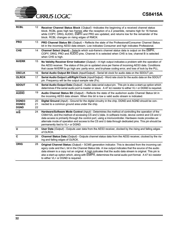
VA+
VL+ = 3 V
VL+ = 5 V
-
-
-
-
-
-
-
-
-
20
60
60
6.3
30.1
46.5
6.6
44.8
76.6
-
-
-
-
-
-
-
-
-
碌A(chǔ)
碌A(chǔ)
碌A(chǔ)
mA
mA
mA
mA
mA
mA
(AGND = DGND = 0 V; all voltages with respect to 0 V.)
Symbol
Min
Typ
Max
Units
Normal Operation
(Note 4)
Supply Current at 48 kHz frame rate
Supply Current at 96 kHz frame rate
Notes: 3. Power Down Mode is defined as RST = LO with all clocks and data lines held static.
4. Normal operation is defined as RST = HI.
DIGITAL INPUT CHARACTERISTICS
Parameters
Input Leakage Current
Differential Input Voltage, RXP0 to RXN0
Symbol
I
in
V
TH
Min
-
-
Typ
鹵1
200
Max
鹵10
-
Units
碌A(chǔ)
mV
DIGITAL INTERFACE SPECIFICATIONS
(AGND = DGND = 0 V; all voltages with respect to 0 V.)
Parameters
High-Level Output Voltage (I
OH
= -3.2 mA)
Low-Level Output Voltage (I
OH
= 3.2 mA)
High-Level Input Voltage, except RX
n
Low-Level Input Voltage, except RX
n
Notes: 5.
(Note 5)
Symbol
V
OH
V
OL
V
IH
V
IL
Min
(VL+) - 1.0
-
2.0
-0.3
Max
-
0.4
(VL+) + 0.3
0.4/0.8
Units
V
V
V
V
At 5V mode, V
IL
= 0.8V (Max), at 3V mode, V
IL
=0.4V (Max).
SWITCHING CHARACTERISTICS
(Inputs: Logic 0 = 0V, Logic 1 = VL+; C
L
= 20 pF)
Parameter
RST pin Low Pulse Width
PLL Clock Recovery Sample Rate Range
RMCK output jitter
RMCK output duty cycle
Notes: 6.
(Note 6)
Symbol
Min
200
8.0
-
40
Typ
-
-
200
50
Max
-
108.0
-
60
Units
碌s
kHz
ps RMS
%
Cycle-to-cycle using 32-96kHz external PLL filter components.
6


 1
1
 2
2
 3
3
 4
4
 5
5
 6
6
 7
7
 8
8
 9
9
 10
10
 11
11
 12
12
 13
13
 14
14
 15
15
 16
16
 17
17
 18
18
 19
19
 20
20
 21
21
 22
22
 23
23
 24
24
 25
25
 26
26
 27
27
 28
28
 29
29
 30
30
 31
31
 32
32
 33
33
 34
34
 35
35
 36
36
 37
37
 38
38
 39
39
 40
40
 41
41
 42
42
