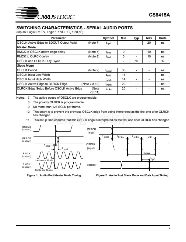
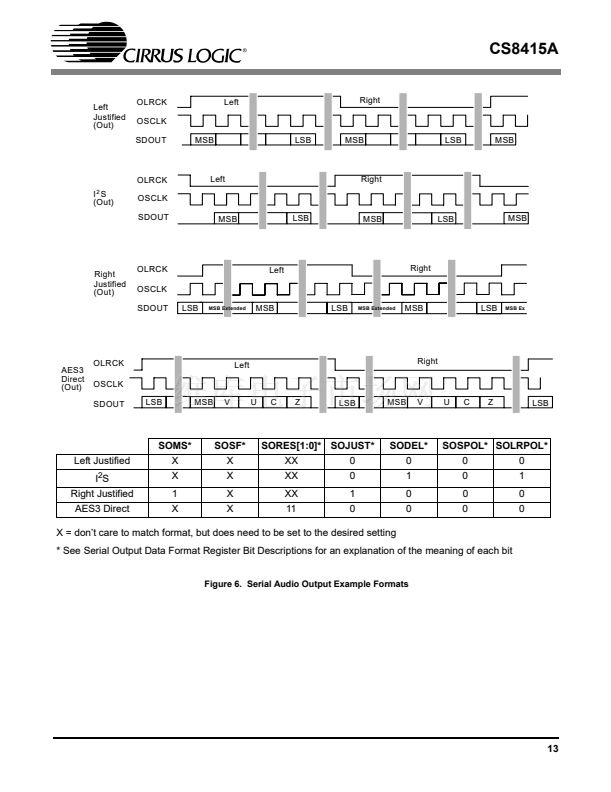
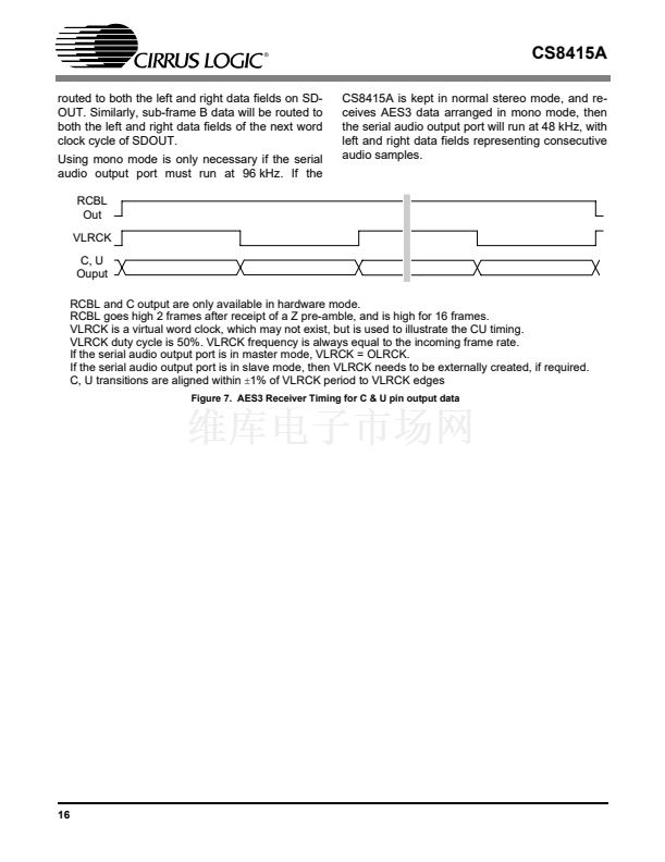
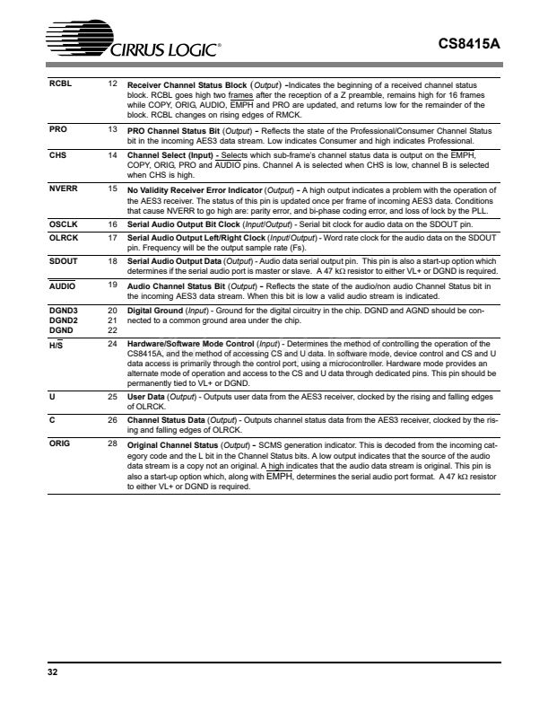
CS8415A
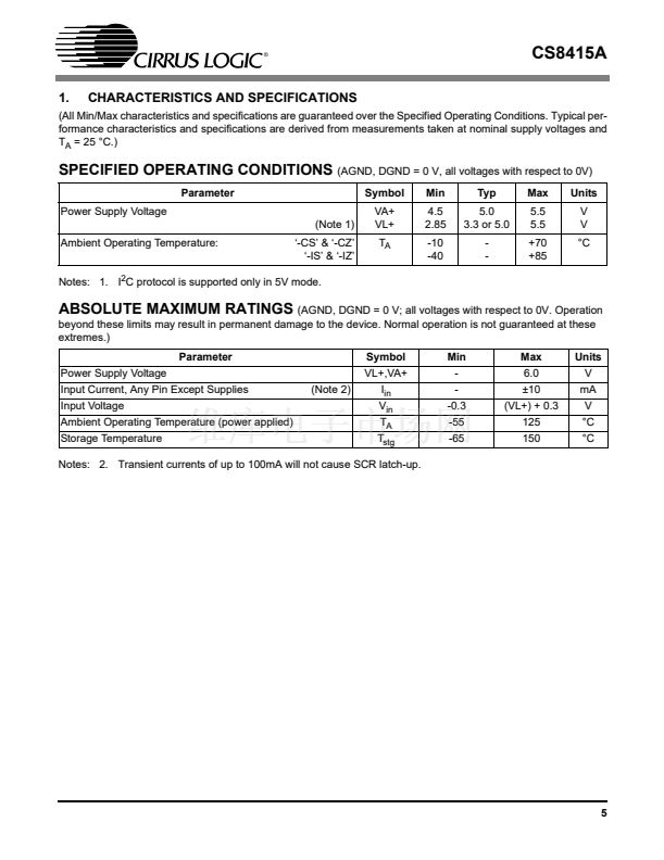
2. TYPICAL CONNECTION DIAGRAM
Ferrite *
Bead
0.1
碌
F
0.1
碌
F
+5V
Analog
Supply *
+3.3V or +5V
Digital
Supply
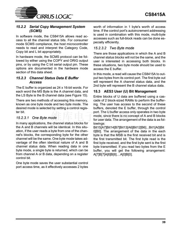
VA+
RXP6
RXP5
RXP4
RXP3
RXP2
RXP1
RXP0
RXN0
CS8415A
VL+
**
AES3/
SPDIF
Sources
OLRCK
OSCLK
SDOUT
3-wire Serial
Audio Input
Device
Clock Control
RMCK
SDA/CDOUT
AD0/CS
SCL/CCLK
AD1/CDIN
INT
U
DGND2
H/S
DGND
Microcontroller
Hardware
Control
EMPH/AD 2
RERR
RST
AGND FILT
RFILT
CFILT
CRIP
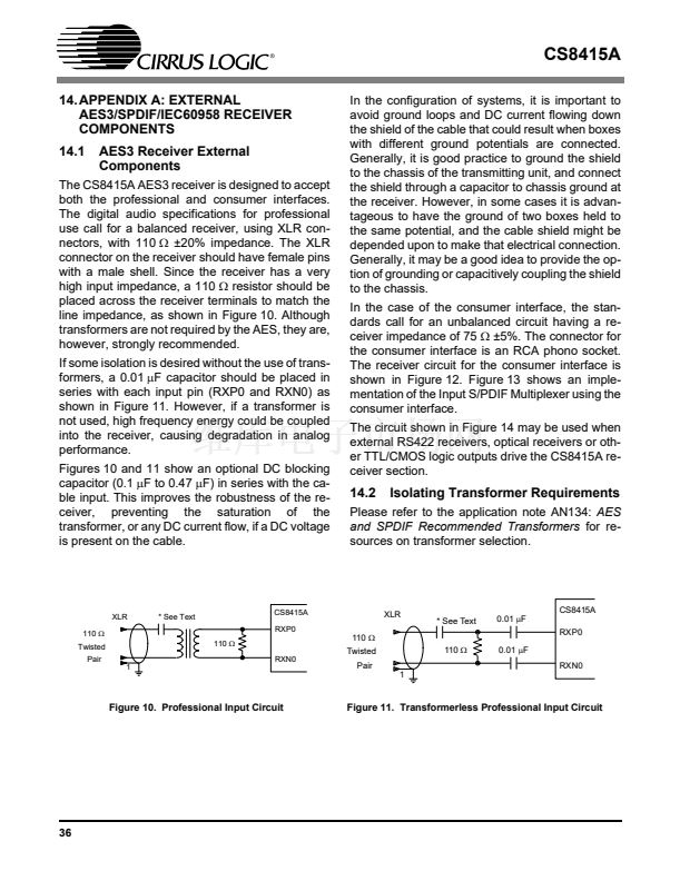
* A separate analog supply is only necessary in applications where RMCK is used
for a jitter sensitive task. For applications where RMCK is not used for a jitter
sensitive task, connect VA+ to VD+ via a ferrite bead. Keep the decoupling
capacitor between VA+ and AGND.
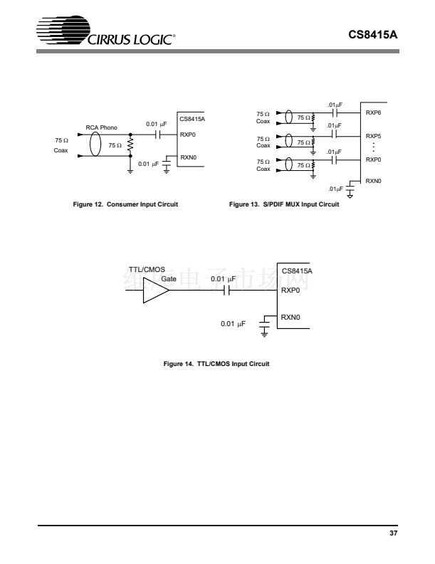
* * Please see section 5.1 "7:1 S/PDIF Input Multiplexer" and Appendix A for typical
input configurations and recommended input circuits.
Figure 5. Recommended Connection Diagram for Software Mode
10


 1
1
 2
2
 3
3
 4
4
 5
5
 6
6
 7
7
 8
8
 9
9
 10
10
 11
11
 12
12
 13
13
 14
14
 15
15
 16
16
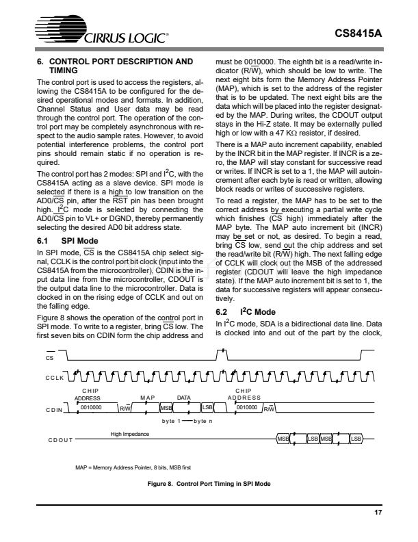 17
17
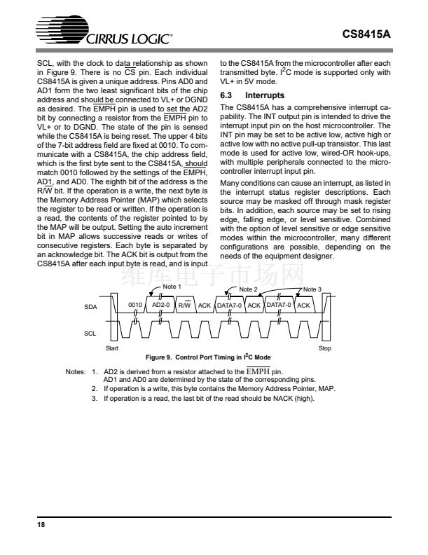 18
18
 19
19
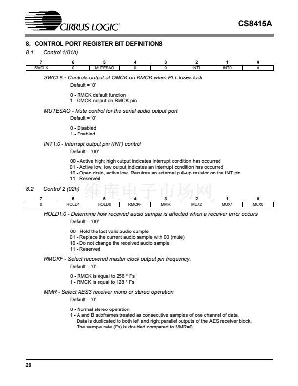 20
20
 21
21
 22
22
 23
23
 24
24
 25
25
 26
26
 27
27
 28
28
 29
29
 30
30
 31
31
 32
32
 33
33
 34
34
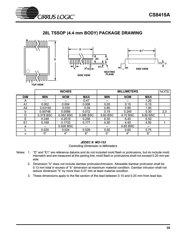 35
35
 36
36
 37
37
 38
38
 39
39
 40
40
 41
41
 42
42
