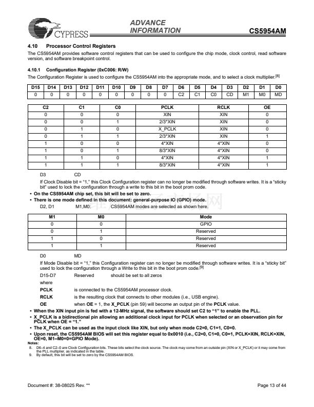
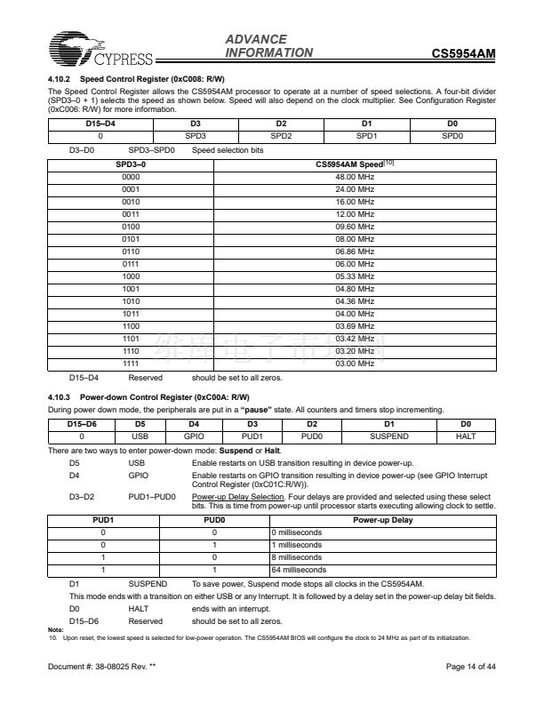
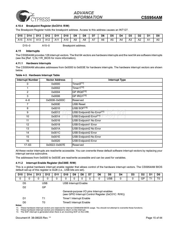
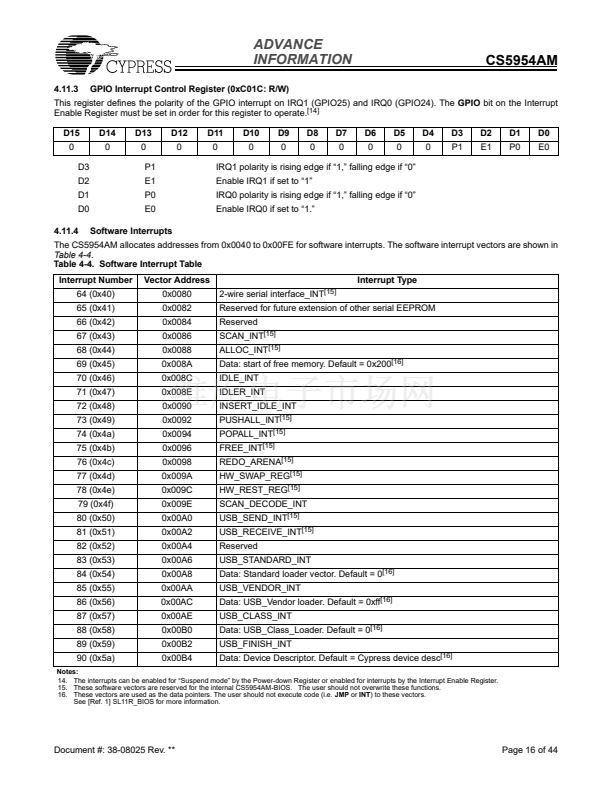
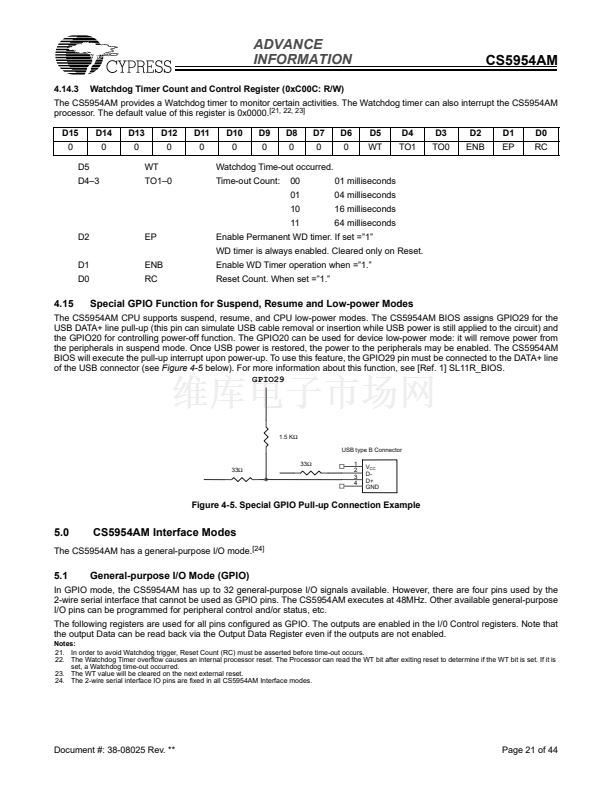
ADVANCE
INFORMATION
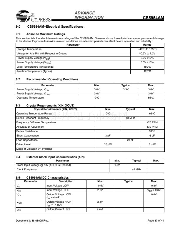
Parameter
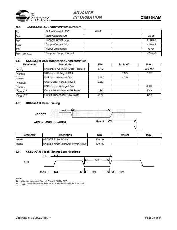
tclk
thigh
tlow
trise
tfall
Description
Clock Period (48 MHz)
Clock HIGH Time
Clock LOW Time
Clock Rise Time
Clock Fall Time
Duty Cycle
鈥?%
Min.
20.0 ns
9 ns
9 ns
Typical
20.8 ns
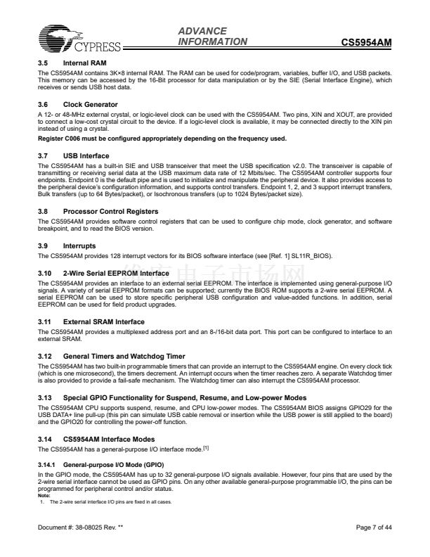
CS5954AM
Max.
11 ns
11 ns
5.0 ns
5.0 ns
+5%
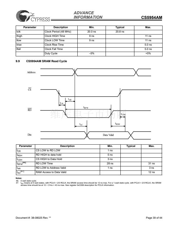
9.9
CS5954AM SRAM Read Cycle
Address
CS
t
AR
t
CR
RD
t
RPW
t
CDH
t
AC
t
RDH
Din
Data Valid
Parameter
t
CR
t
RDH
t
CDH
t
RPW[46]
t
AR
t
AC[47]
Description
CS LOW to RD LOW
RD HIGH to data hold
CS HIGH to Data Hold
RD LOW Time
RD LOW to Address Valid
RAM Access to Data Valid
Min.
1 ns
5 ns
3 ns
28 ns
1 ns
Typical
Max.
31 ns
3 ns
12 ns
Notes:
46. 0 wait state cycle.
47. t
AC
means at 0 wait states, with PCLK = 2/3 RCLK, the SRAM access time should be 12 ns max. For a 1-wait state cycle, with PCLK = 2/3 RCLK, the SRAM
access time should be at 12 + 31ns = 43 ns max. See register 0xC006 description for PCLK information.
Document #: 38-08025 Rev. **
Page 39 of 44


 1
1
 2
2
 3
3
 4
4
 5
5
 6
6
 7
7
 8
8
 9
9
 10
10
 11
11
 12
12
 13
13
 14
14
 15
15
 16
16
 17
17
 18
18
 19
19
 20
20
 21
21
 22
22
 23
23
 24
24
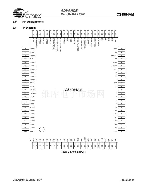 25
25
 26
26
 27
27
 28
28
 29
29
 30
30
 31
31
 32
32
 33
33
 34
34
 35
35
 36
36
 37
37
 38
38
 39
39
 40
40
 41
41
 42
42
 43
43
 44
44
