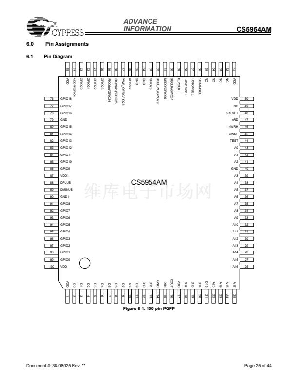
ADVANCE
INFORMATION
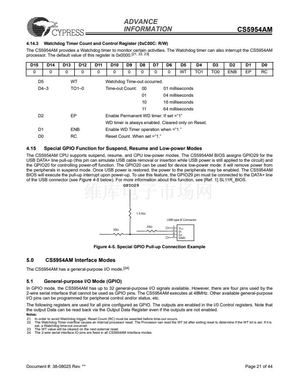
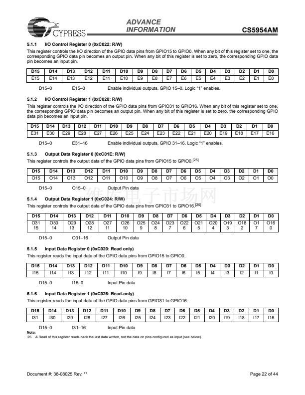
5.1.1
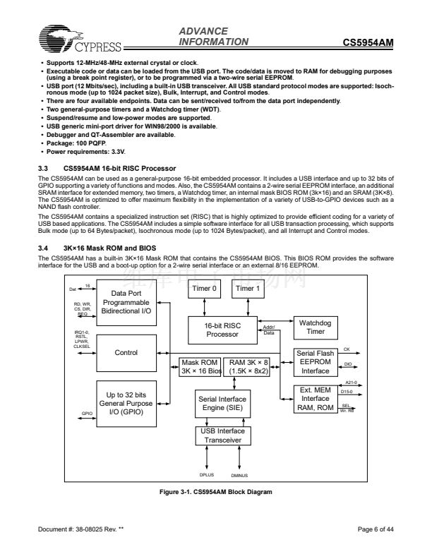
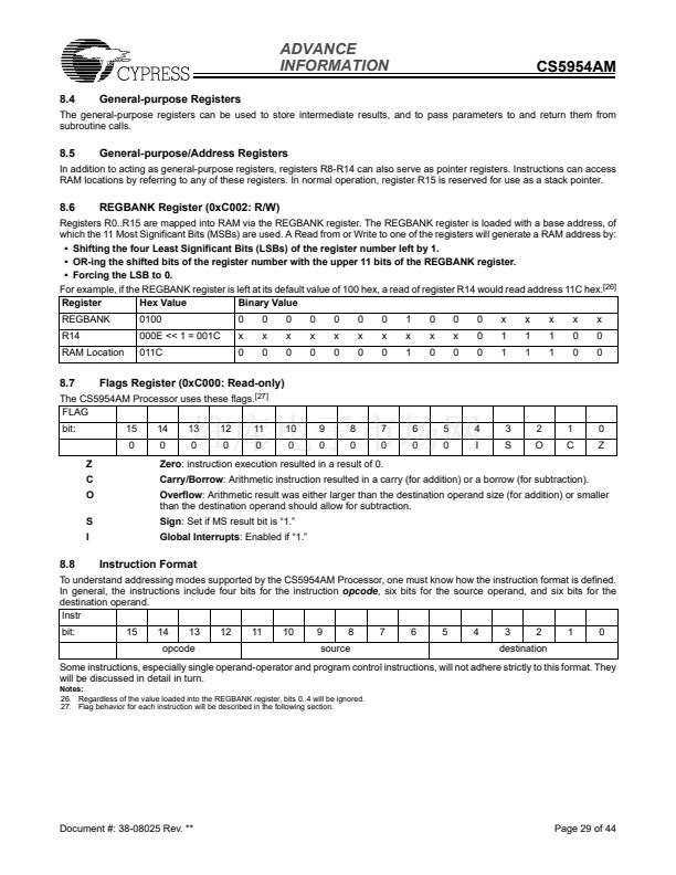
I/O Control Register 0 (0xC022: R/W)
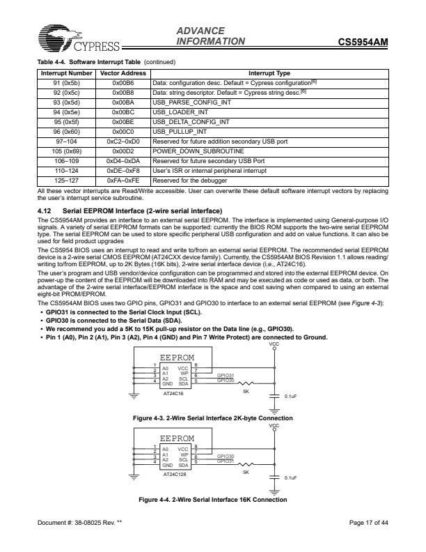
CS5954AM
This register controls the I/O direction of the GPIO data pins from GPIO15 to GPIO0. When any bit of this register set to one, the
corresponding GPIO data pin becomes an output pin. When any bit of this register is set to zero, the corresponding GPIO data
pin becomes an input pin.
D15
E15
D14
E14
D13
E13
D12
E12
D11
E11
D10
E10
D9
E9
D8
E8
D7
E7
D6
E6
D5
E5
D4
E4
D3
E3
D2
E2
D1
E1
D0
E0
D15鈥?
5.1.2
E15鈥?
Enable individual outputs, GPIO 15鈥?. Logic 鈥?鈥?enables.
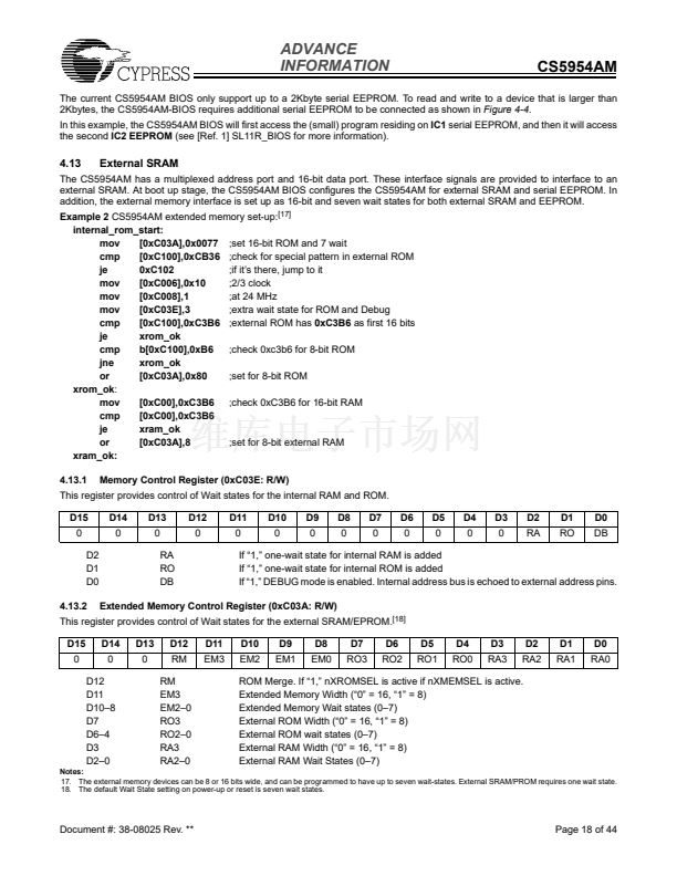
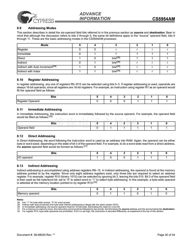
I/O Control Register 1 (0xC028: R/W)
This register controls the I/O direction of the GPIO data pins from GPIO31 to GPIO16. When any bit of this register set to one,
the corresponding GPIO data pin becomes an output pin. When any bit of this register is set to zero, the corresponding GPIO
data pin becomes an input pin.
D15
E31
D14
E30
D15鈥?
5.1.3
D13
E29
D12
E28
E31鈥?6
D11
E27
D10
E26
D9
E25
D8
E24
D7
E23
D6
E22
D5
E21
D4
E20
D3
E19
D2
E18
D1
E17
D0
E16
Enable individual outputs, GPIO 31鈥?6. Logic 鈥?鈥?enables.
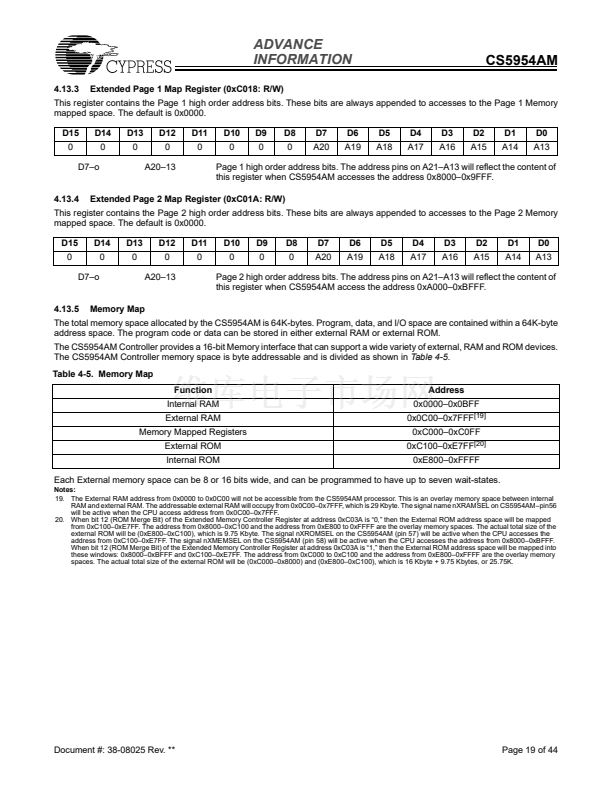
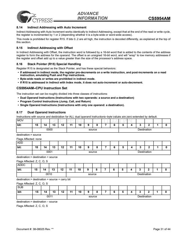
Output Data Register 0 (0xC01E: R/W)
This register controls the output data of the GPIO data pins from GPIO15 to GPIO0.
[25]
D15
O15
D14
O14
D13
O13
D12
O12
D11
O11
D10
O10
D9
O9
D8
O8
D7
O7
D6
O6
D5
O5
D4
O4
D3
O3
D2
O2
D1
O1
D0
O0
D15鈥?
5.1.4
O15鈥?
Output Pin data
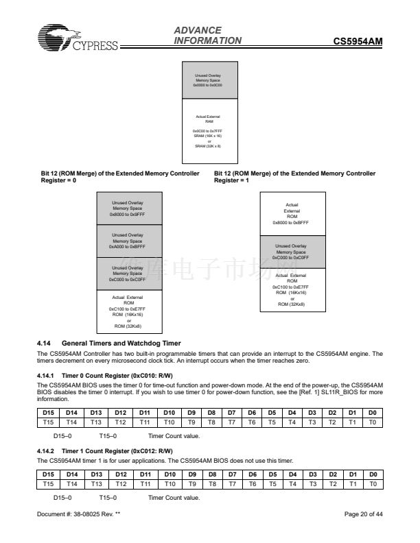
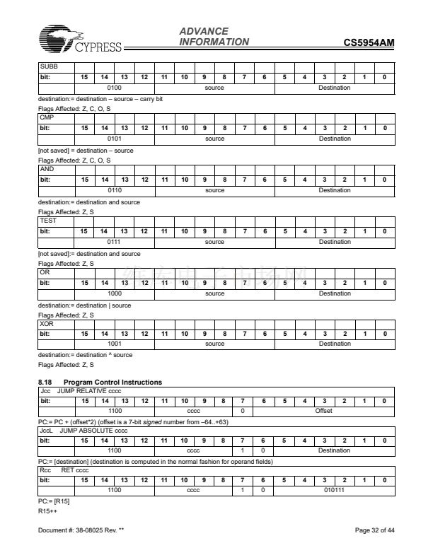
Output Data Register 1 (0xC024: R/W)
This register controls the output data of the GPIO data pins from GPIO31 to GPIO16.
[25]
D15
O31
15
D14
O30
14
D13
O29
13
D12
O28
12
D11
O27
11
D10
O26
10
D9
O25
9
D8
O24
8
D7
O23
7
D6
O22
6
D5
O21
5
D4
O20
4
D3
O19
3
D2
O18
2
D1
O1
7
D0
O16
0
D15鈥?
5.1.5
O31鈥?6
Output Pin data
Input Data Register 0 (0xC020: Read only)
This register reads the input data of the GPIO data pins from GPIO15 to GPIO0.
D15
I15
D14
I14
D15鈥?
5.1.6
D13
I13
I15鈥?
D12
I12
D11
I11
D10
I10
D9
I9
D8
I8
D7
I7
D6
I6
D5
I5
D4
I4
D3
I3
D2
I2
D1
I1
D0
I0
Input Pin data
Input Data Register 1 (0xC026: Read-only)
This register reads the input data of the GPIO data pins from GPIO31 to GPIO16.
D15
I31
D14
I30
D15鈥?
D13
I29
D12
I28
D11
I27
D10
I26
D9
I25
D8
I24
D7
I23
D6
I22
D5
I21
D4
I20
D3
I19
D2
I18
D1
I17
D0
I16
I31鈥?6
Input Pin data
Note:
25. A Read of this register reads back the last data written, not the data on pins configured as input (see below).
Document #: 38-08025 Rev. **
Page 22 of 44


 1
1
 2
2
 3
3
 4
4
 5
5
 6
6
 7
7
 8
8
 9
9
 10
10
 11
11
 12
12
 13
13
 14
14
 15
15
 16
16
 17
17
 18
18
 19
19
 20
20
 21
21
 22
22
 23
23
 24
24
 25
25
 26
26
 27
27
 28
28
 29
29
 30
30
 31
31
 32
32
 33
33
 34
34
 35
35
 36
36
 37
37
 38
38
 39
39
 40
40
 41
41
 42
42
 43
43
 44
44
