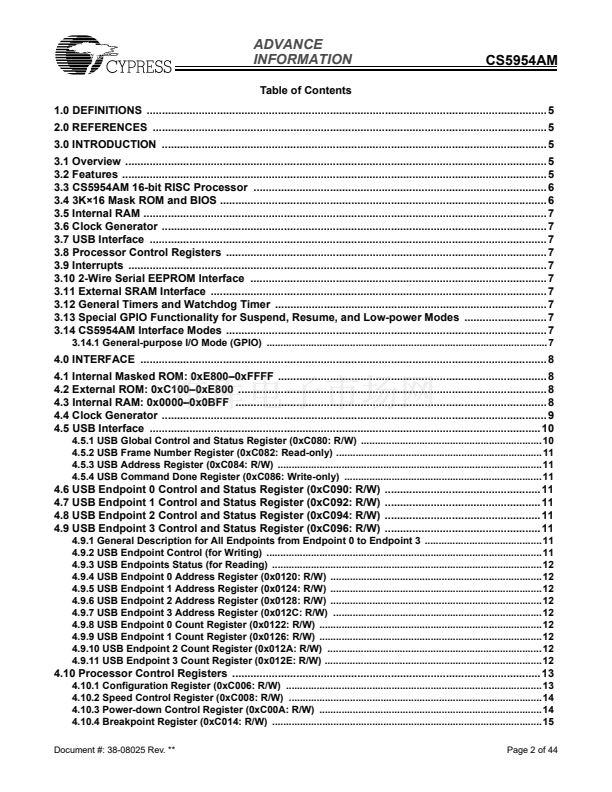
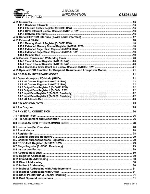
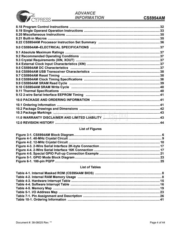
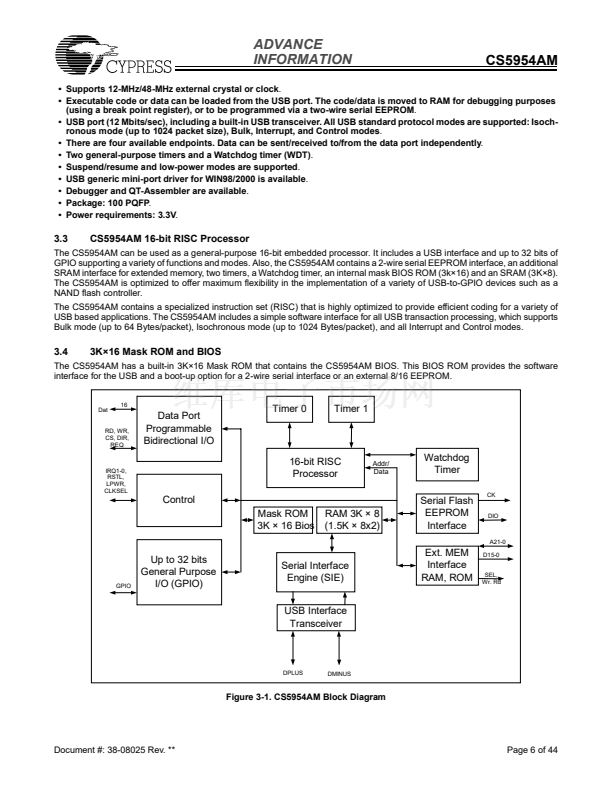
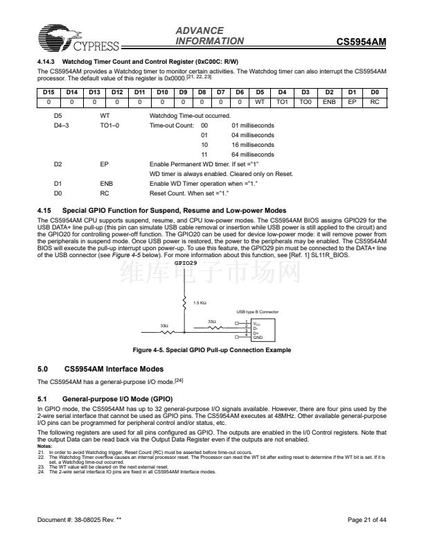
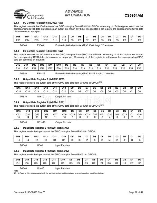
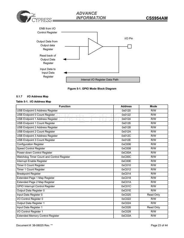
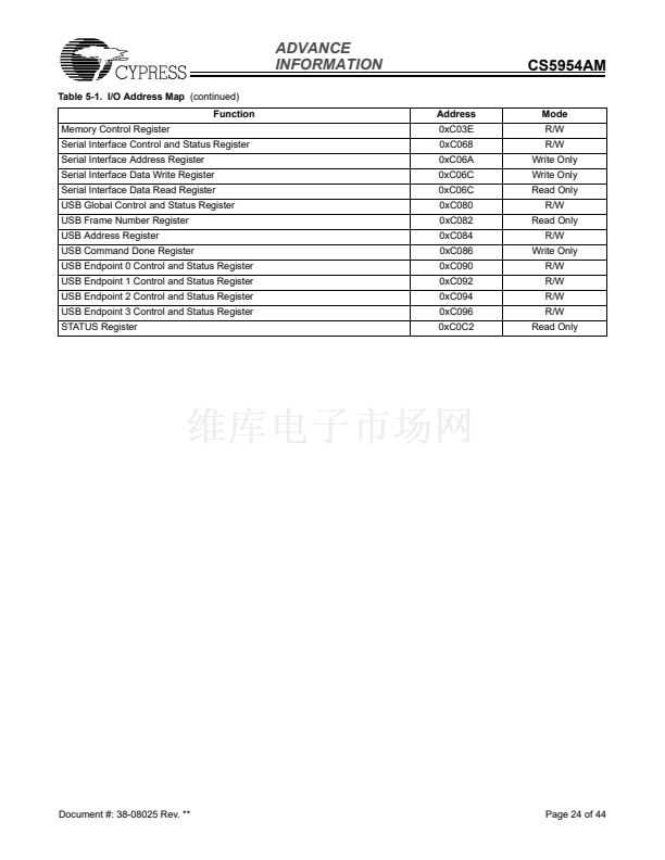
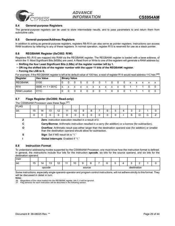
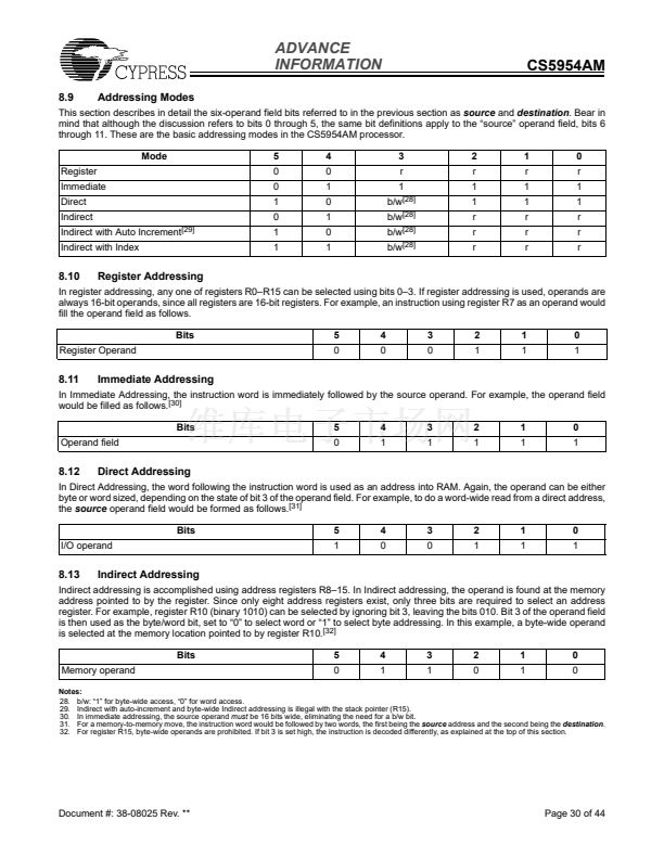
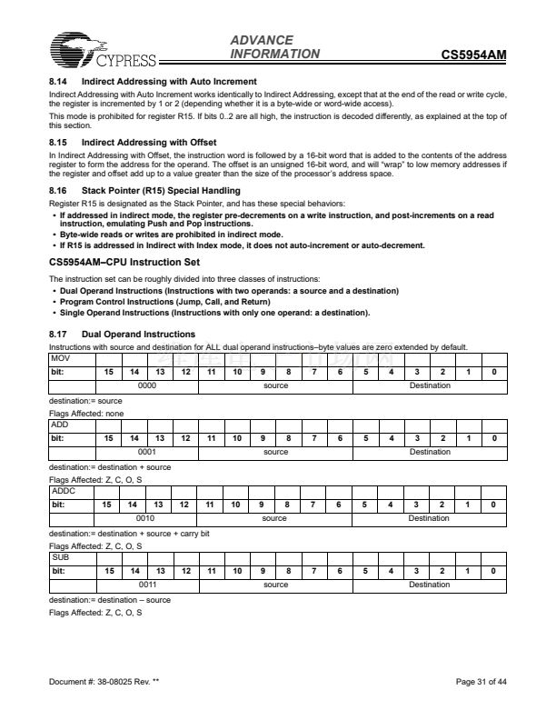
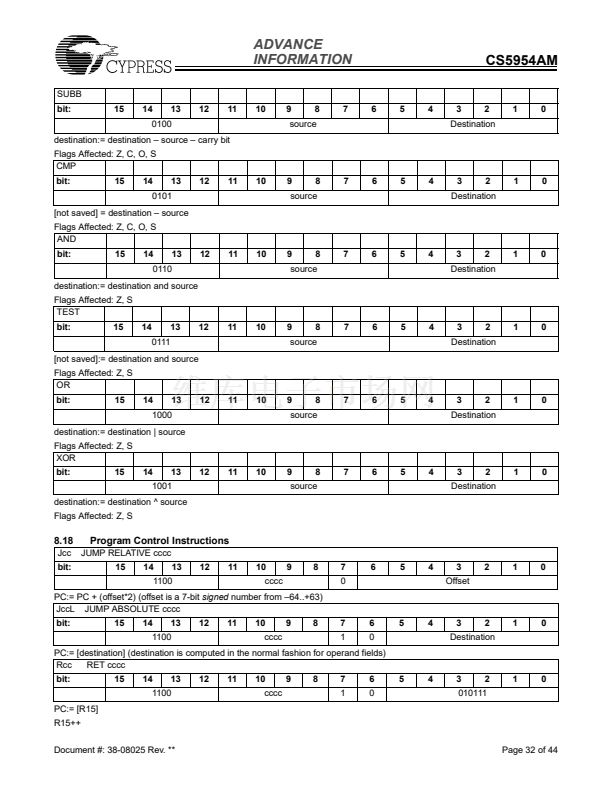
鈥?/div>
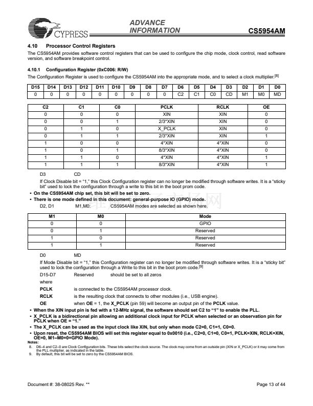
is connected to the CS5954AM processor clock.
is the resulting clock that connects to other modules (i.e., USB engine).
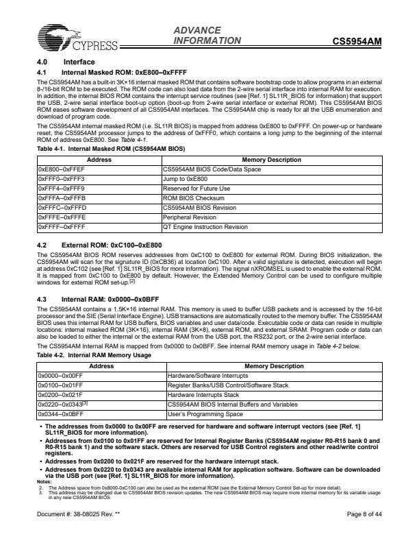
Reserved
should be set to all zeros
OE
when
OE
= 1, the
X_PCLK
(pin 59) will become an output pin of the
PCLK
value.
When the XIN input pin is fed with a 12-MHz signal, the software should set C2 to 鈥?鈥?to enable the PLL.
X_PCLK is a bidirectional pin allowing an additional clock input for PCLK when selected or an observation pin for
PCLK when OE = 鈥?.鈥?/div>
The X_PCLK can be used as the input clock like XIN, but only when mode C2=0, C1=1, C0=0.
Upon reset, the CS5954AM BIOS will set this register equal to 0x0010 (i.e., C2=0, C1=0, C0=1, PCLK=XIN, RCLK=XIN,
OE=0, M1鈥揗0=0=GPIO Mode).
Notes:
8. D6鈥? and C2鈥? are Clock Configuration bits. These bits select the clock source. The clock may come from an outside pin (XIN or X_PCLK) or it may come from
the PLL multiplier, as indicated in the table.
9. By default, this bit will be set to zero by the CS5954AM BIOS.
Document #: 38-08025 Rev. **
Page 13 of 44


 1
1
 2
2
 3
3
 4
4
 5
5
 6
6
 7
7
 8
8
 9
9
 10
10
 11
11
 12
12
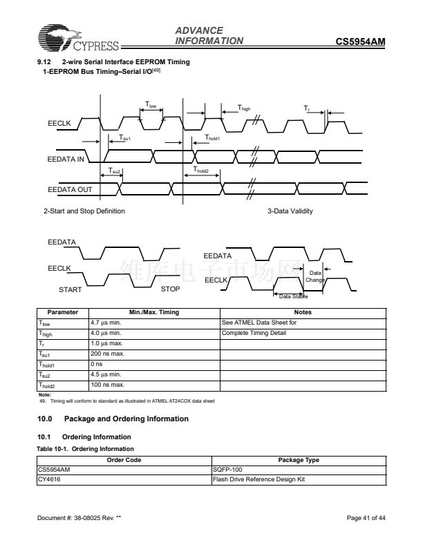
 13
13
 14
14
 15
15
 16
16
 17
17
 18
18
 19
19
 20
20
 21
21
 22
22
 23
23
 24
24
 25
25
 26
26
 27
27
 28
28
 29
29
 30
30
 31
31
 32
32
 33
33
 34
34
 35
35
 36
36
 37
37
 38
38
 39
39
 40
40
 41
41
 42
42
 43
43
 44
44
