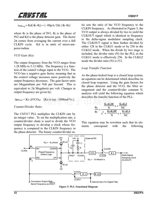
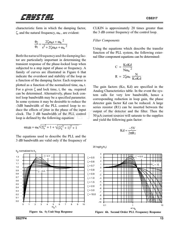
CDB5317
amplitude so that distortion products become neg-
ligible. This allows an accurate measurement of
the noise floor.
More complex analysis such as intermodulation
distortion measurements can be accomplished
with the addition of another sine-wave generator.
are supplied on the board to connect the +5, -5,
and ground power lines. A good quality low rip-
ple, low noise supply will give the best
performance. The +5 V supply can also be used
for VL and should be connected between the VL
board jack and the power supply, as opposed to
connecting the VL jack straight to the +5V jack.
The +5V jack is the positive power source for the
CS5317 IC whereas the VL jack supplies power
to all the digital ICs. Care should be taken that
noise is not coupled between VL and +5V; how-
ever, supply noise is generally not a problem with
the CS5317 since the on-chip decimation filter
will remove any interference outside of its pass-
band. The +5 and -5 V supply lines are filtered on
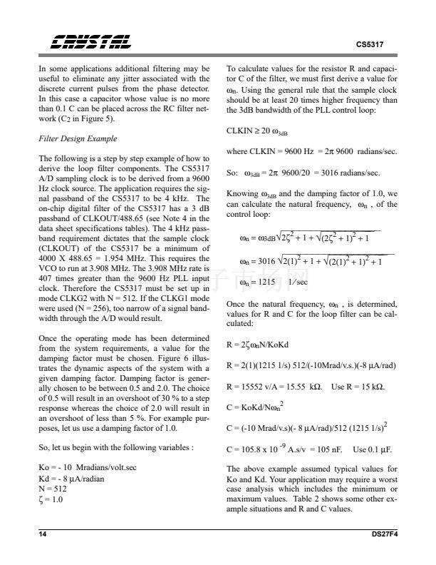
CIRCUIT DESCRIPTION
Figure 2 illustrates the CS5317 A/D converter IC
circuit connections. The chip operates off of
鹵5V.
These voltages are supplied from a power source
external to the evaluation board. Binding posts
TP6
VL
D1
TP10
+5V
6.8v
D3
C19
C17
0.22碌F
R10
10k
R2
200
R1*
51
AIN
R11
1.2k
C18
0.01
碌F
NPO
TP8
C9
10碌F
C8
0.1
碌F
1
VA+
C5
C4
VL
0.1
碌F
10
碌F
R7
10
2
VD+
3
+ C6
10
碌F
R5
10 k
DOUT (fig. 3)
CLKOUT (fig. 3)
DATA (fig. 3)
R6
10 k
C7
0.1
碌F
17
PHDT
18
VCOIN
9
CLKIN
DOE
CLKIN
CLKIN (fig.6)
11
U6
AIN
8
DOUT
5
CLKOUT
6
DATA
16
RST
R9
10 k
12 REFBUF
C14
0.1
碌F
15
AGND
VA-
14
R8
10
C15
MODE
7
CLKG1
CLKG2 P2
CLKOR
TP7
GND
D2
TP9
-5V
C16
CS5317
DGND
VD-
10
4
C13
C12 +
10
碌F
6.8v
10碌F 0.1
碌F
0.1
碌F
* Remove for logic gate CLKIN source
Figure 2. Analog-to-Digital Converter
DS27DB3
27


 1
1
 2
2
 3
3
 4
4
 5
5
 6
6
 7
7
 8
8
 9
9
 10
10
 11
11
 12
12
 13
13
 14
14
 15
15
 16
16
 17
17
 18
18
 19
19
 20
20
 21
21
 22
22
 23
23
 24
24
 25
25
 26
26
 27
27
 28
28
 29
29
 30
30
 31
31
 32
32
