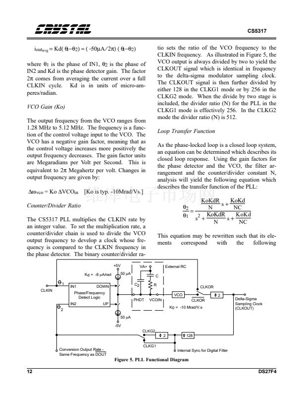
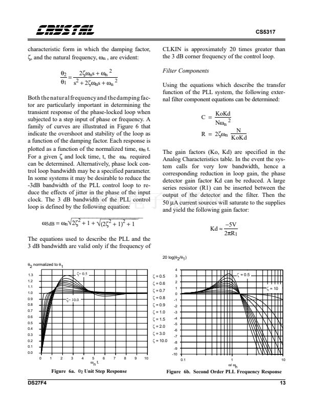
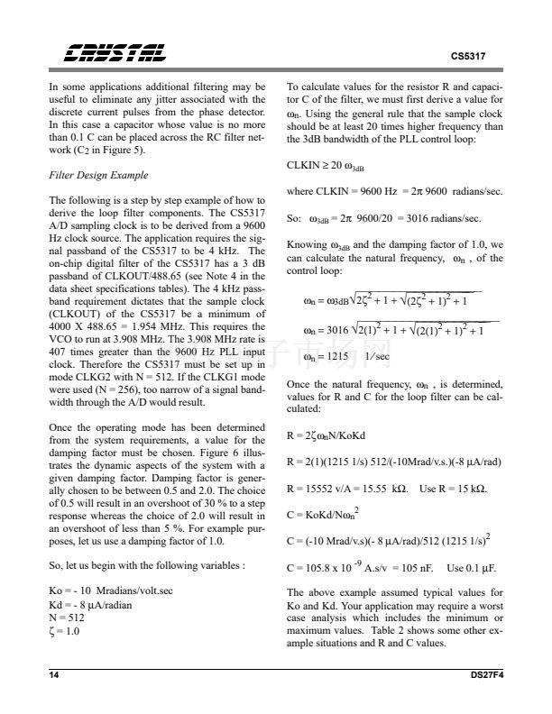
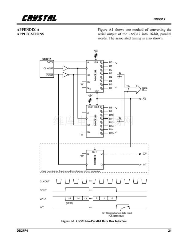
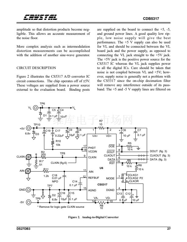
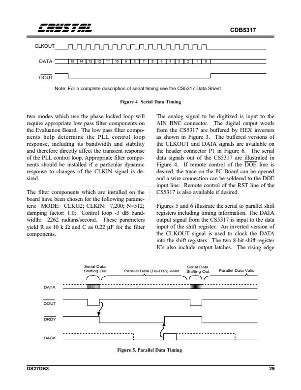
Parallel Digital I/O Interface".
鈥?/div>
A software routine to collect the data and per-
form a Fast Fourier Transform (FFT).
The evaluation board includes filter components
for the on-chip phase locked loop. The compo-
nents are adequate for testing if the CLKIN signal
has little or no phase-jitter. If the CDB5317 board
is being tested as part of a system which generates
a CLKIN which contains jitter, the PLL filter
components may need to be optimized for your
system (see the CS5317 data sheet).
Set-up for evaluation is straightforward. First de-
cide the operating mode and place the jumper on
the board for the proper selection. Then decide
whether the filter components for the phase
locked loop are adequate or whether they should
be changed for your evaluation. The PLL will
lock on a steady clock input with the filter as it is.
Connect the necessary 5 V (CMOS compatible)
CLKIN signal for the application. Use the sine-
wave generator to supply the analog signal to the
CDB5317. Apply the analog input and CLKIN
signals only when the evaluation board is pow-
ered up. Converted data will then appear at the
header on the CDB5317. The header should be
connected to the digital data acquisition board in
the PC through an IDC 40 pin connector and ca-
ble. The software routine should collect the data
from the CDB5317 and run a standard 1024 point
Fast Fourier Transform (FFT). Such an analysis
results in a plot similar to Figure 1. This plot re-
sulted from using a 1kHz input signal and a
Blackman-Harris window for the FFT.
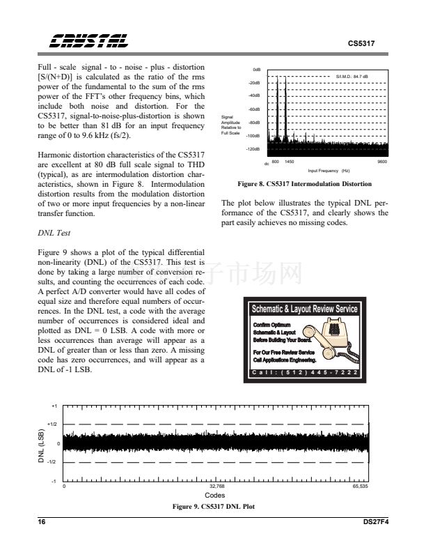
The signal to noise and signal to total harmonic
distortion characteristics of the CS5317 may be
easily measured in this way. The signal to total
harmonic distortion value for a particular input is
the ratio of the RMS value of the input signal and
the sum of the RMS values of the harmonics
shown in the diagram. The dynamic range of the
CS5317 can be measured by reducing the input
0dB
-20dB
-40dB
Signal
-60dB
Amplitude
Relative to
Full Scale -80dB
-100dB
Sampling Rate: 19.2 kHz
Full Scale:
鹵 2.75 V
S/(N+D): 81.39 dB
-120dB
dc
1 kHz
Input Frequency
9.6 kHz
Figure 1. FFT Plot Example
26
DS27DB3


 1
1
 2
2
 3
3
 4
4
 5
5
 6
6
 7
7
 8
8
 9
9
 10
10
 11
11
 12
12
 13
13
 14
14
 15
15
 16
16
 17
17
 18
18
 19
19
 20
20
 21
21
 22
22
 23
23
 24
24
 25
25
 26
26
 27
27
 28
28
 29
29
 30
30
 31
31
 32
32
