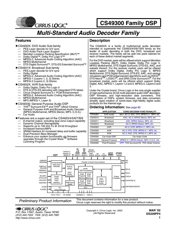
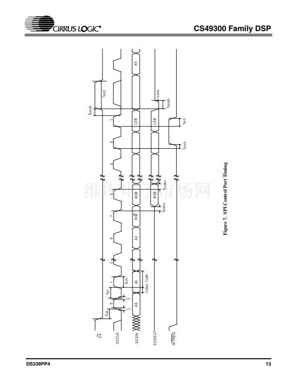
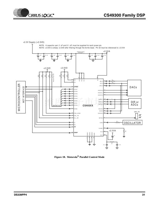
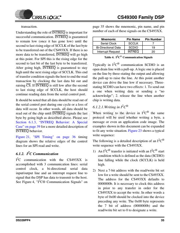
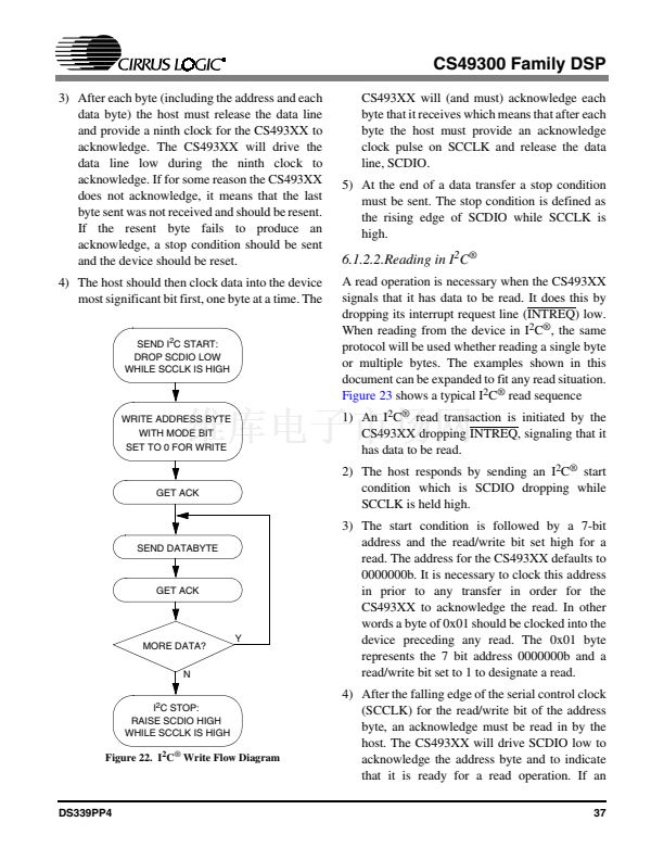
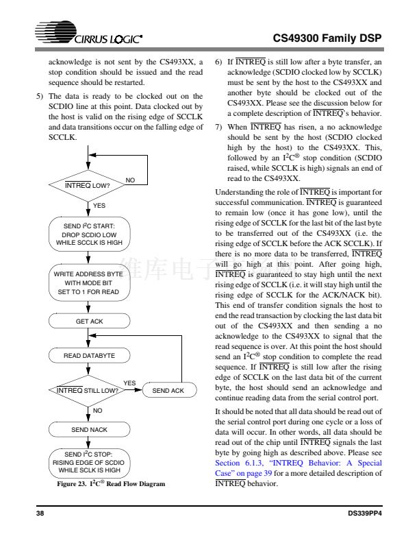
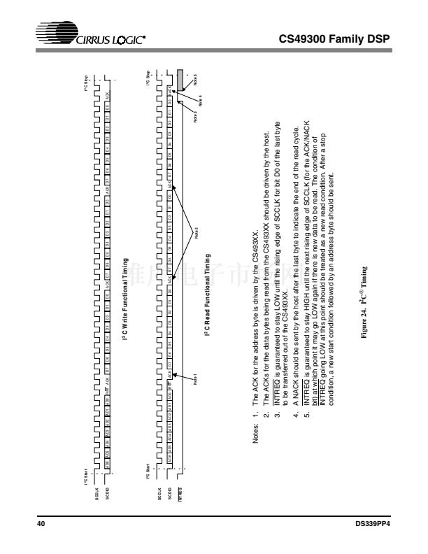
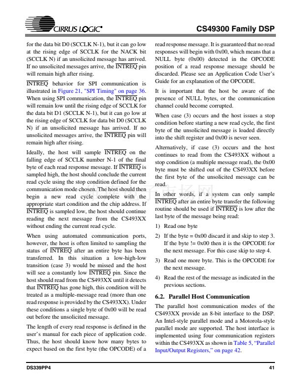
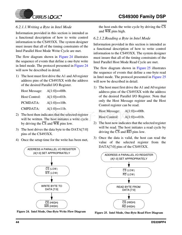
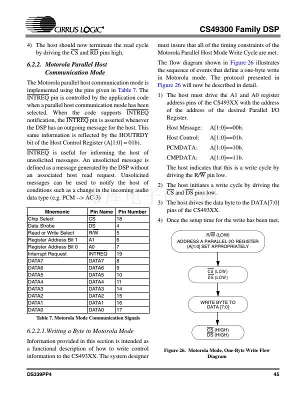
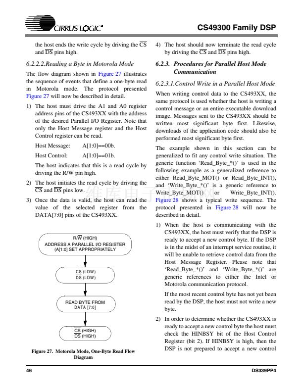
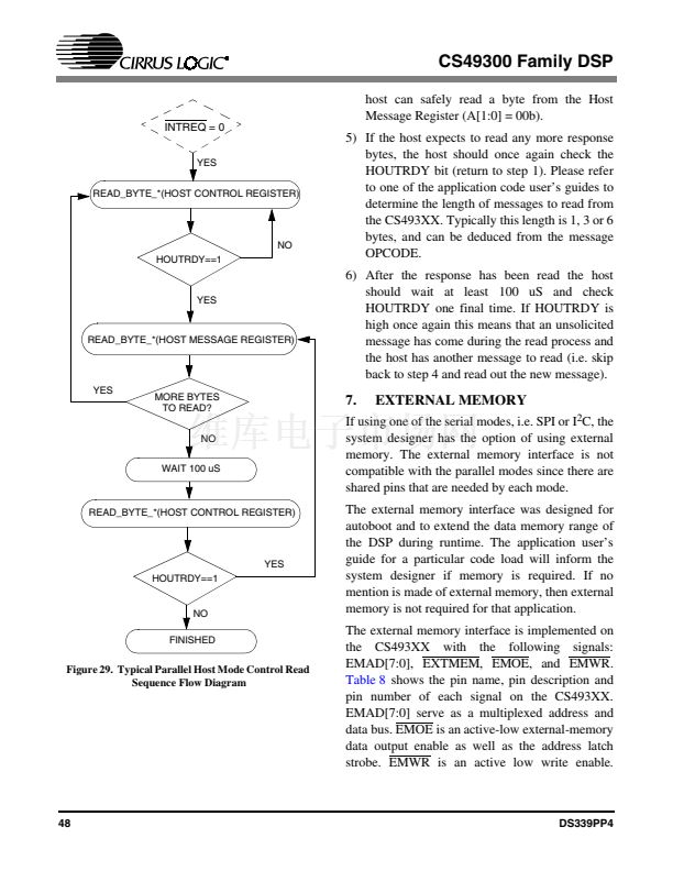
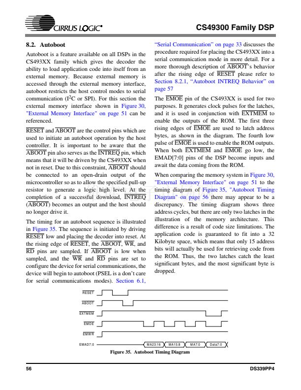
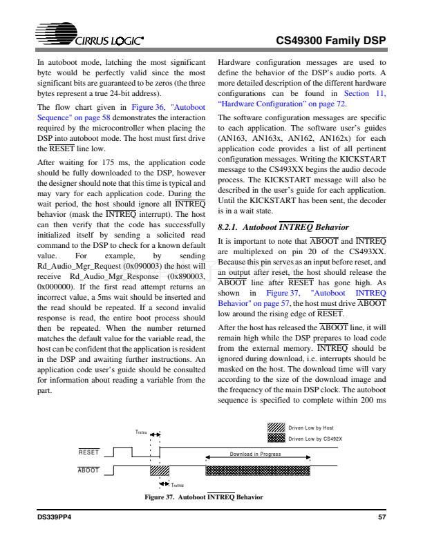
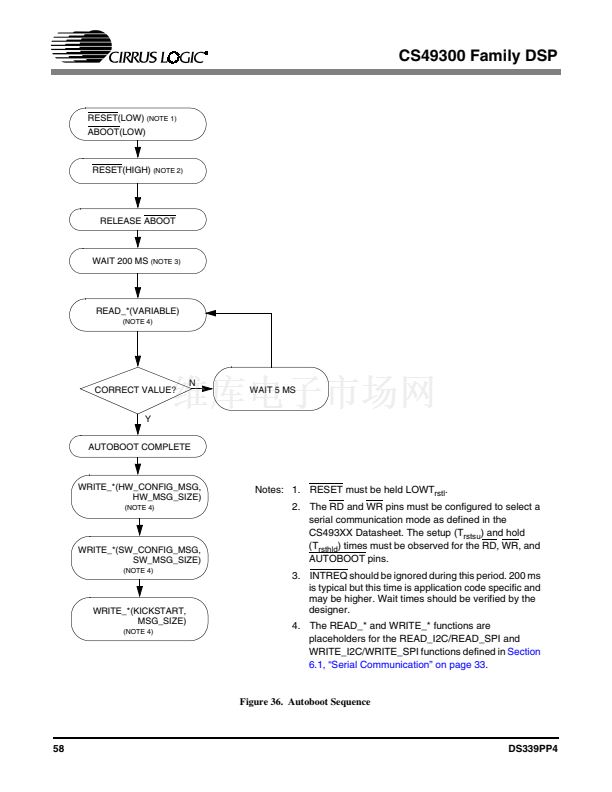
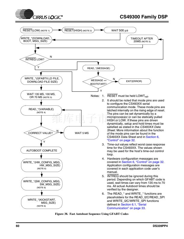
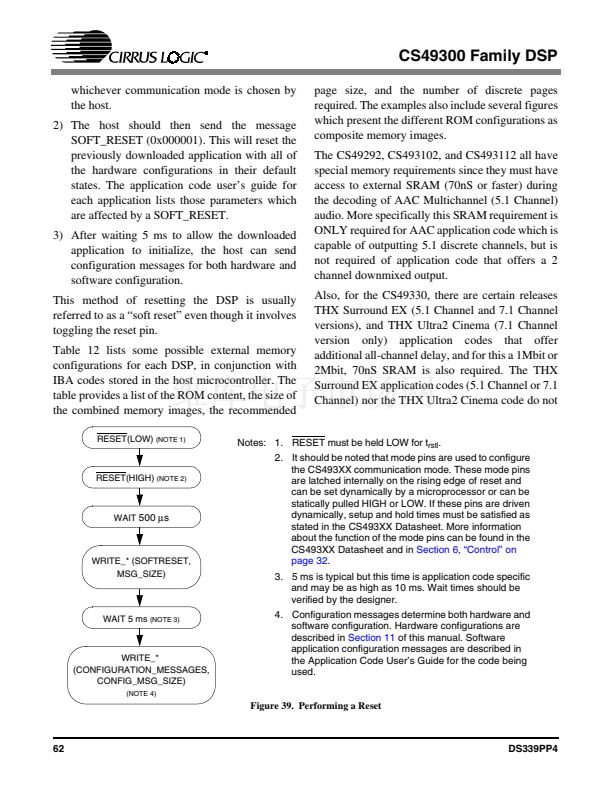
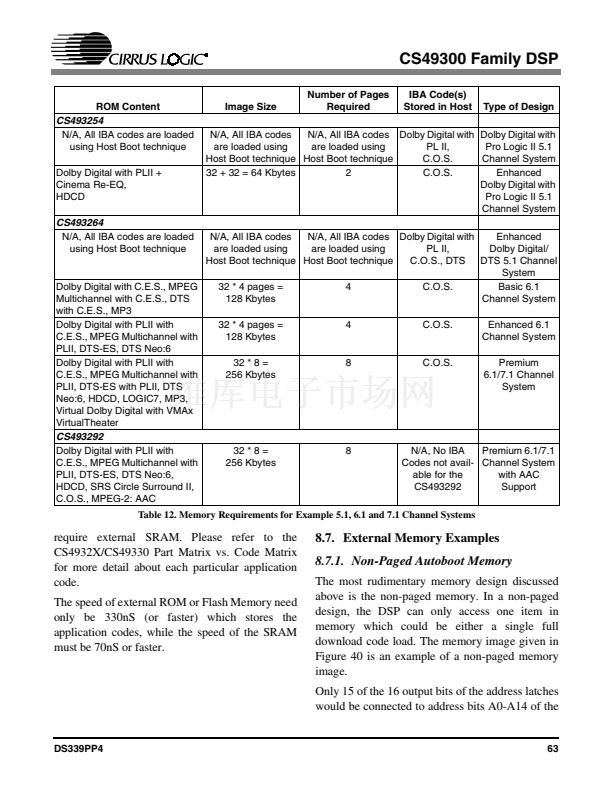
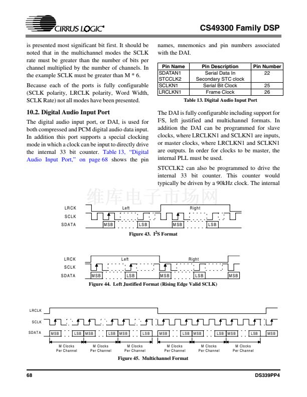
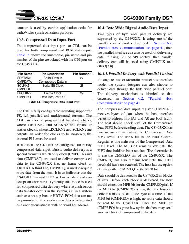
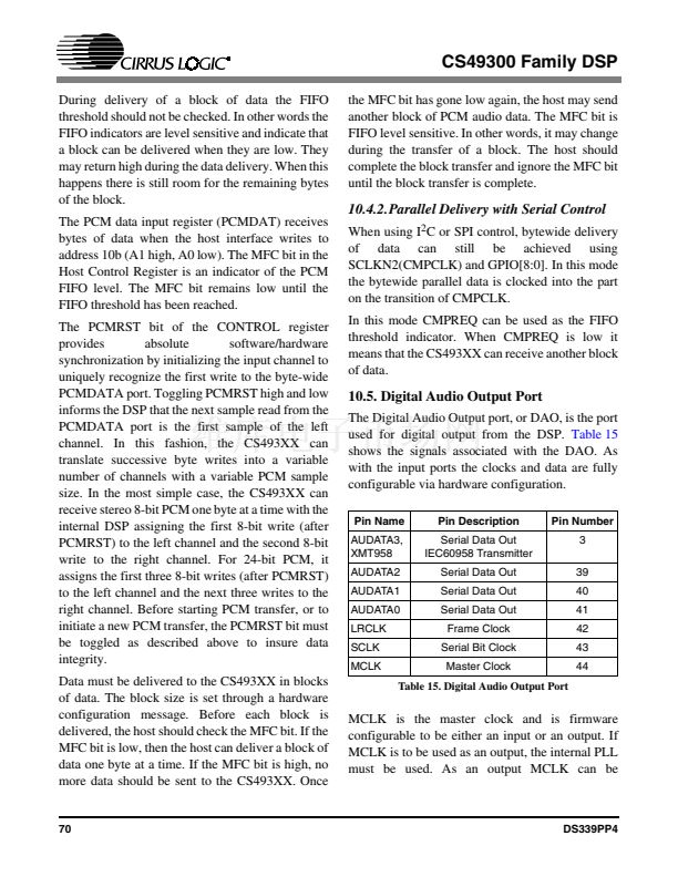
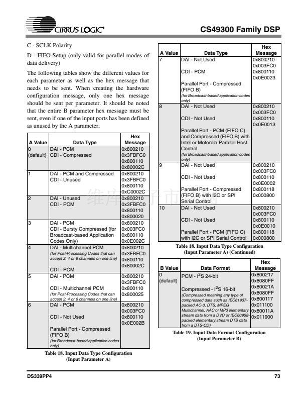
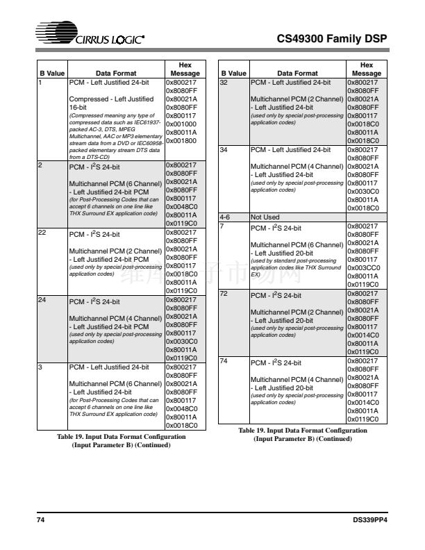
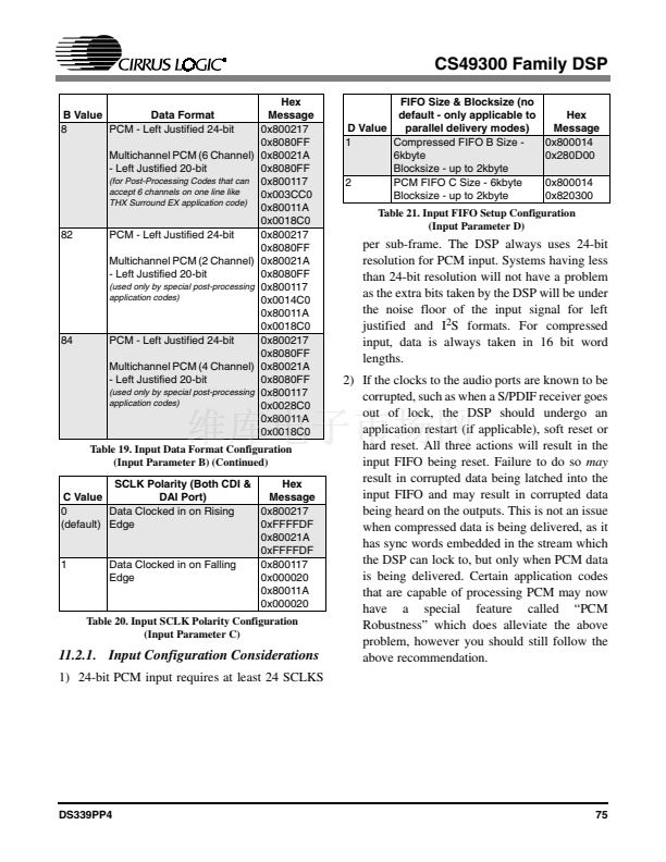
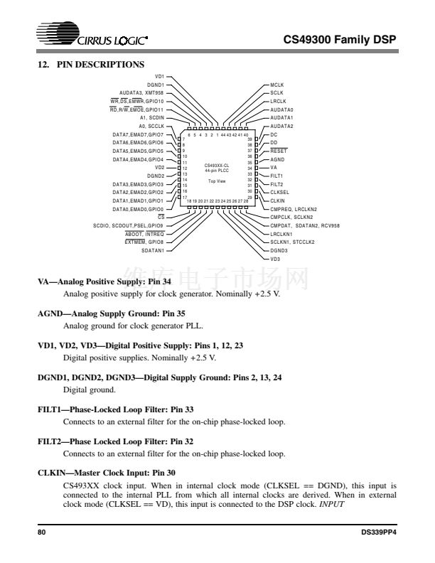
CS49300 Family DSP
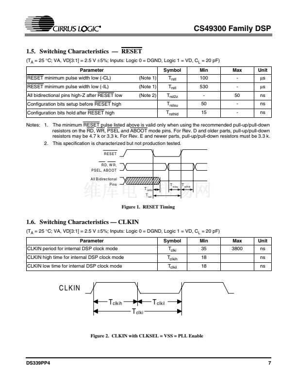
1.5. Switching Characteristics 鈥?RESET
(T
A
= 25
擄C;
VA, VD[3:1] = 2.5 V
鹵5%;
Inputs: Logic 0 = DGND, Logic 1 = VD, C
L
= 20 pF)
Parameter
RESET minimum pulse width low (-CL)
RESET minimum pulse width low (-IL)
All bidirectional pins high-Z after RESET low
Configuration bits setup before RESET high
Configuration bits hold after RESET high
(Note 1)
(Note 1)
(Note 2)
Symbol
T
rstl
T
rstl
T
rst2z
T
rstsu
T
rsthld
Min
100
530
-
50
15
Max
-
-
50
-
-
Unit
碌s
碌s
ns
ns
ns
Notes: 1. The minimum RESET pulse listed above is valid only when using the recommended pull-up/pull-down
resistors on the RD, WR, PSEL and ABOOT mode pins. For Rev. D and older parts, pull-up/pull-down
resistors may be 4.7 k or 3.3 k. For Rev. E and newer parts, pull-up/pull-down resistors must be 3.3 k.
2. This specification is characterized but not production tested.
RESET
RD, W R,
P S E L, A B O O T
A ll B idirectional
P ins
T
rst2z
T
rstl
T
rstsu
T
rsthld
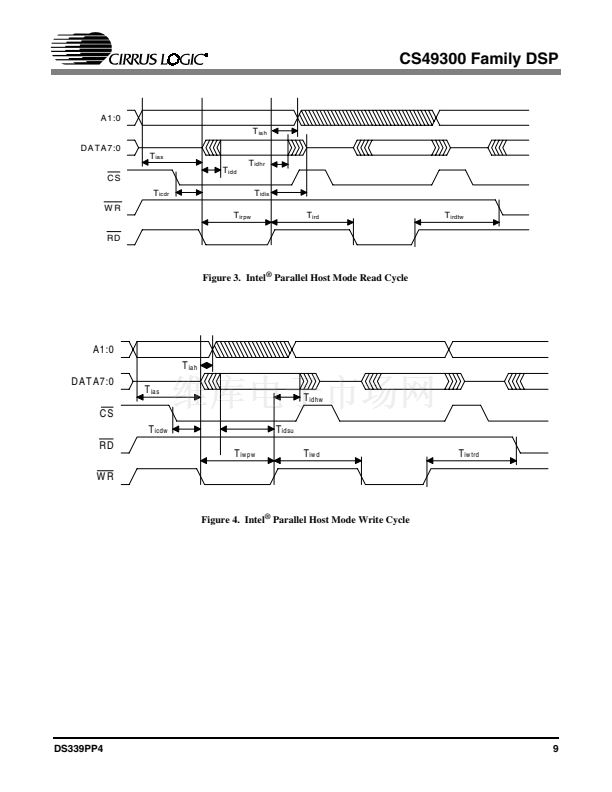
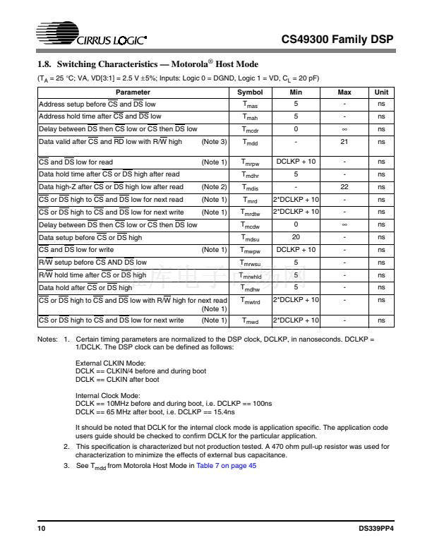
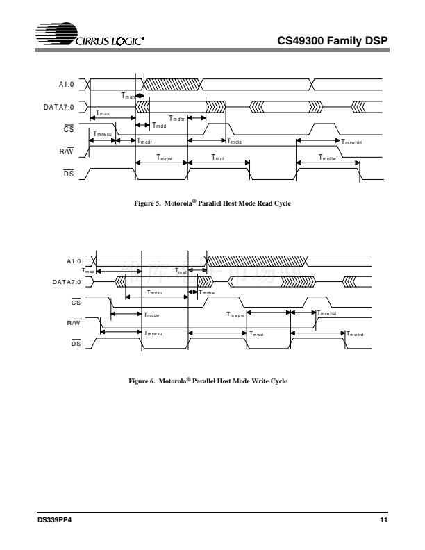
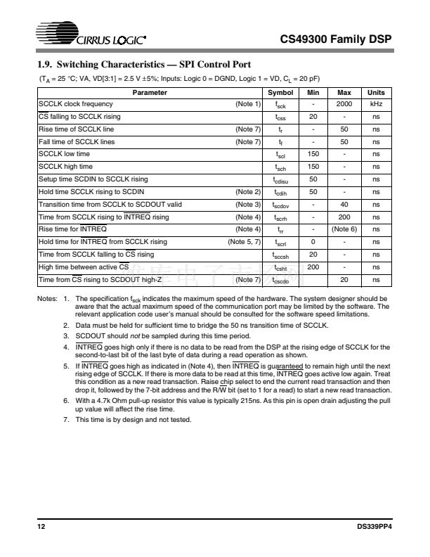
Figure 1. RESET Timing
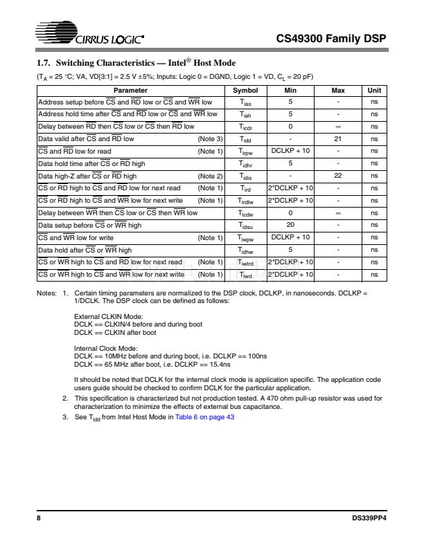
1.6. Switching Characteristics 鈥?CLKIN
(T
A
= 25
擄C;
VA, VD[3:1] = 2.5 V
鹵5%;
Inputs: Logic 0 = DGND, Logic 1 = VD, C
L
= 20 pF)
Parameter
CLKIN period for internal DSP clock mode
CLKIN high time for internal DSP clock mode
CLKIN low time for internal DSP clock mode
Symbol
T
clki
T
clkih
T
clkil
Min
35
18
18
Max
3800
Unit
ns
ns
ns
C L K IN
T
clkih
T
clki
T
clkil
Figure 2. CLKIN with CLKSEL = VSS = PLL Enable
DS339PP4
7


 1
1
 2
2
 3
3
 4
4
 5
5
 6
6
 7
7
 8
8
 9
9
 10
10
 11
11
 12
12
 13
13
 14
14
 15
15
 16
16
 17
17
 18
18
 19
19
 20
20
 21
21
 22
22
 23
23
 24
24
 25
25
 26
26
 27
27
 28
28
 29
29
 30
30
 31
31
 32
32
 33
33
 34
34
 35
35
 36
36
 37
37
 38
38
 39
39
 40
40
 41
41
 42
42
 43
43
 44
44
 45
45
 46
46
 47
47
 48
48
 49
49
 50
50
 51
51
 52
52
 53
53
 54
54
 55
55
 56
56
 57
57
 58
58
 59
59
 60
60
 61
61
 62
62
 63
63
 64
64
 65
65
 66
66
 67
67
 68
68
 69
69
 70
70
 71
71
 72
72
 73
73
 74
74
 75
75
 76
76
 77
77
 78
78
 79
79
 80
80
 81
81
 82
82
 83
83
 84
84
 85
85
 86
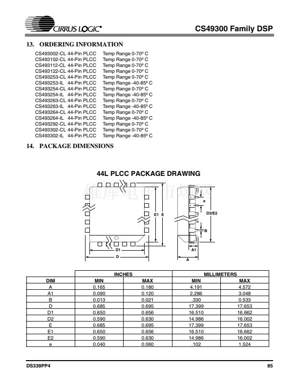
86
