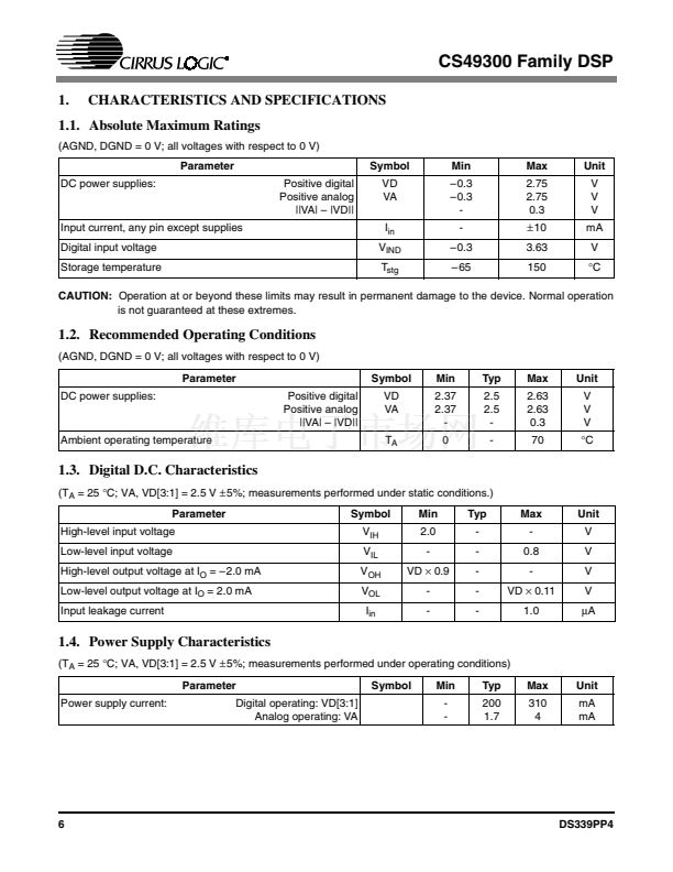
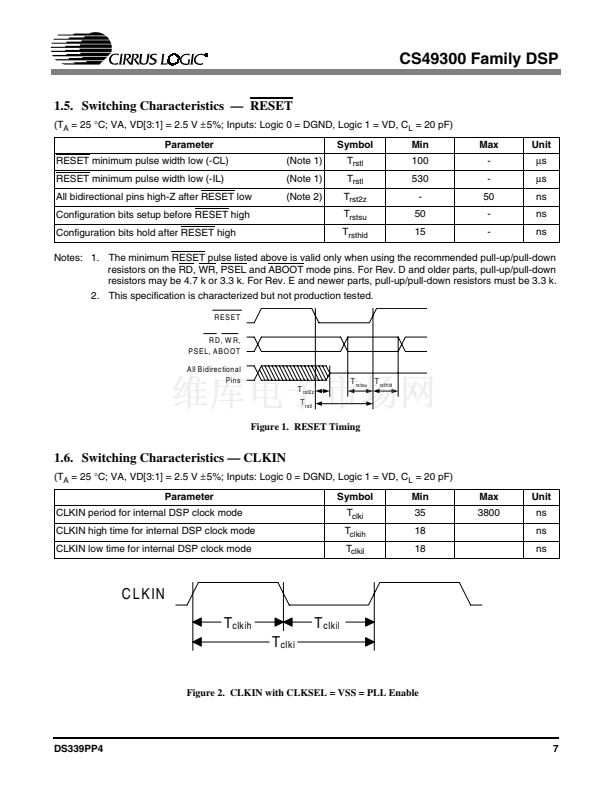
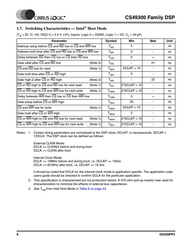
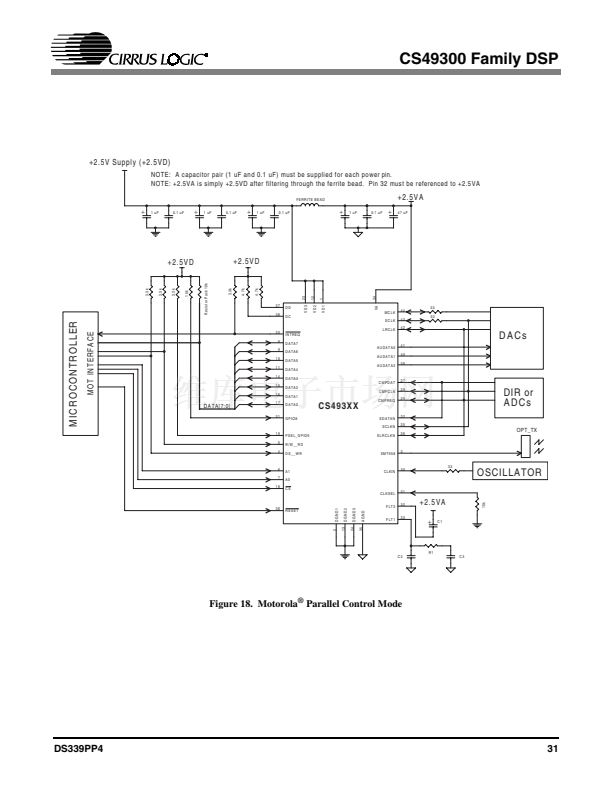
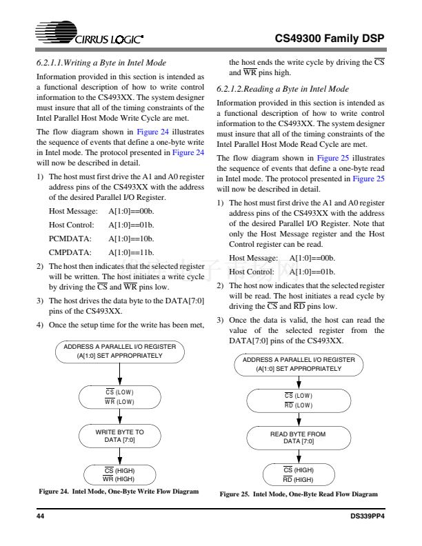
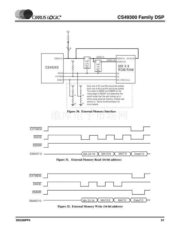
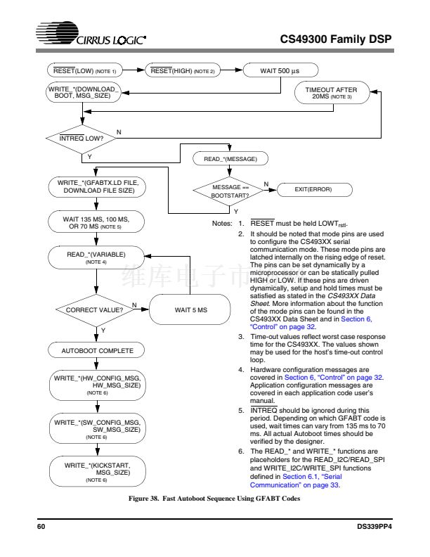
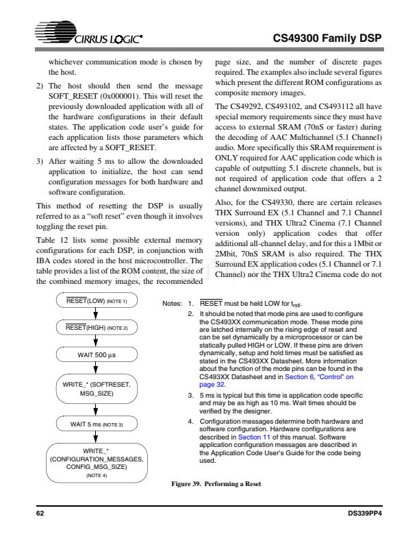
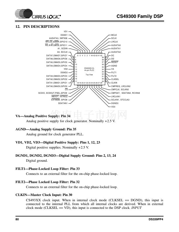
CS49300 Family DSP
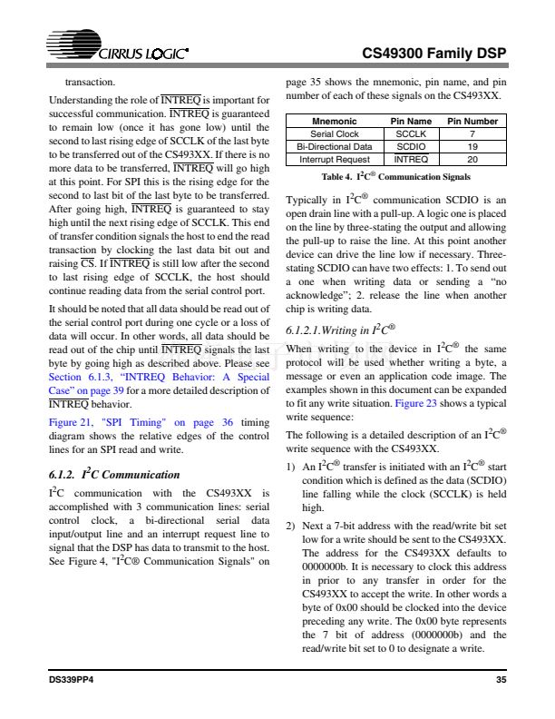
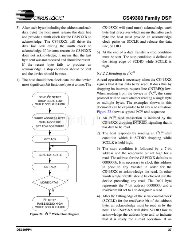
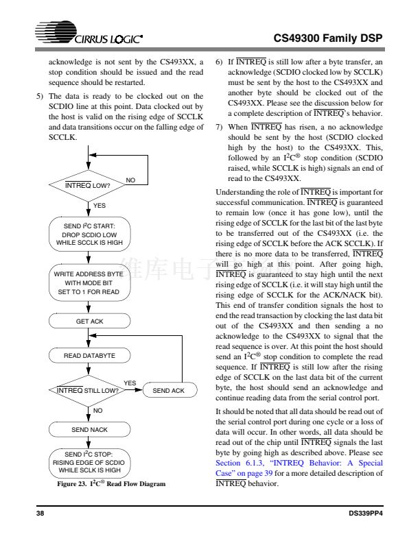
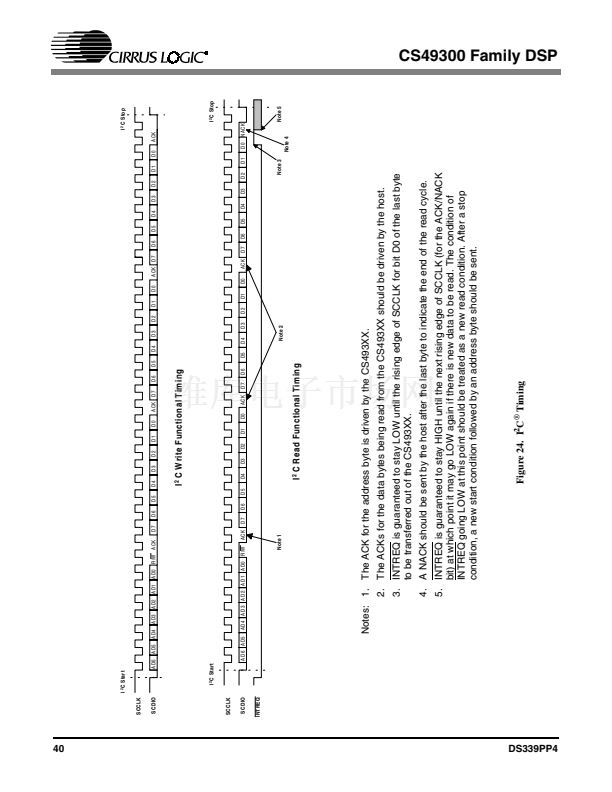
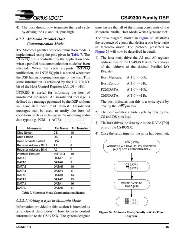
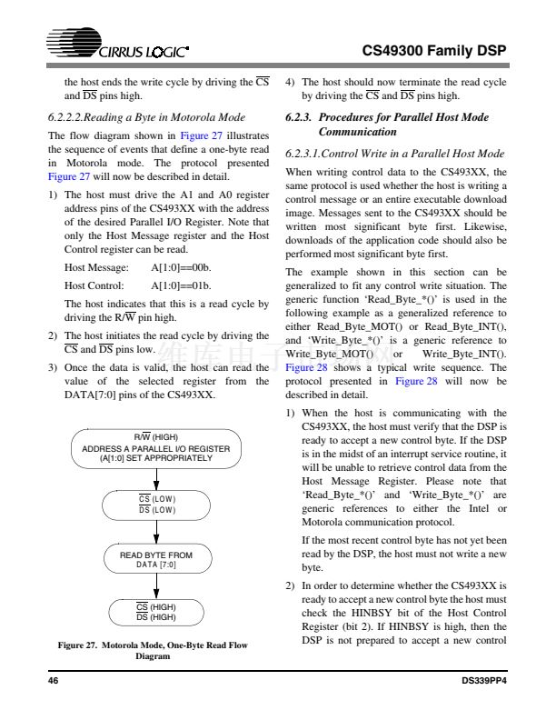
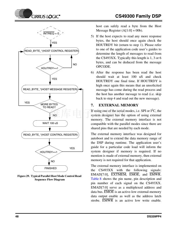
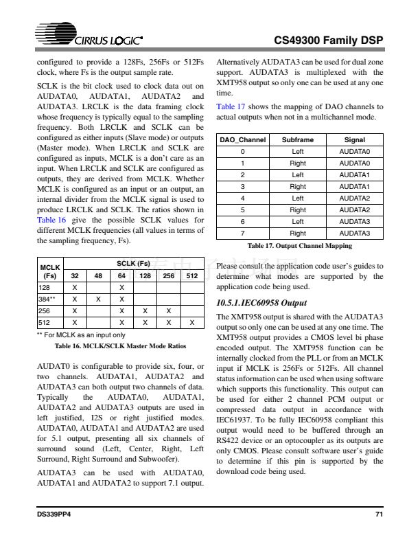
4) The host should now terminate the read cycle
by driving the CS and RD pins high.
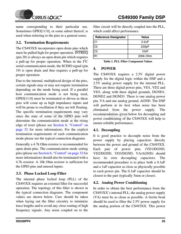
must insure that all of the timing constraints of the
Motorola Parallel Host Mode Write Cycle are met.
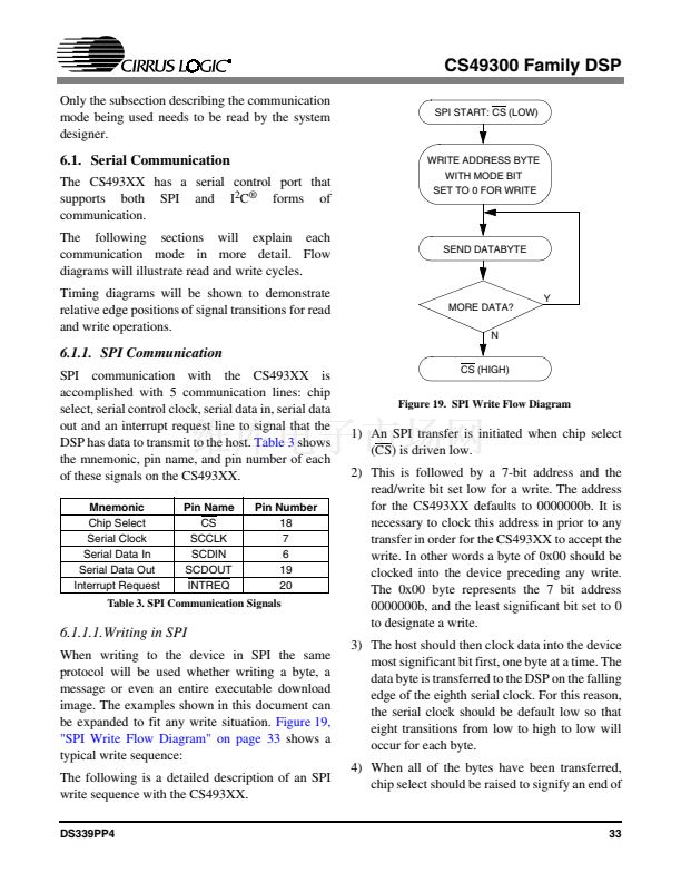
The flow diagram shown in
Figure 26
illustrates
the sequence of events that define a one-byte write
in Motorola mode. The protocol presented in
Figure 26
will now be described in detail.
1) The host must drive the A1 and A0 register
address pins of the CS493XX with the address
of the address of the desired Parallel I/O
Register.
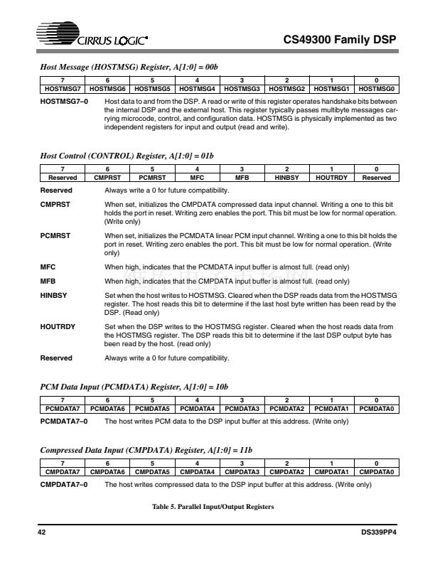
Host Message:
Host Control:
PCMDATA:
CMPDATA:
A[1:0]==00b.
A[1:0]==01b.
A[1:0]==10b.
A[1:0]==11b.
6.2.2. Motorola Parallel Host
Communication Mode
The Motorola parallel host communication mode is
implemented using the pins given in
Table 7.
The
INTREQ pin is controlled by the application code
when a parallel host communication mode has been
selected. When the code supports INTREQ
notification, the INTREQ pin is asserted whenever
the DSP has an outgoing message for the host. This
same information is reflected by the HOUTRDY
bit of the Host Control Register (A[1:0] = 01b).
INTREQ is useful for informing the host of
unsolicited messages. An unsolicited message is
defined as a message generated by the DSP without
an associated host read request. Unsolicited
messages can be used to notify the host of
conditions such as a change in the incoming audio
data type (e.g. PCM --> AC-3)
Mnemonic
Chip Select
Data Strobe
Read or Write Select
Register Address Bit 1
Register Address Bit 0
Interrupt Request
DATA7
DATA6
DATA5
DATA4
DATA3
DATA2
DATA1
DATA0
Pin Name
CS
DS
R/W
A1
A0
INTREQ
DATA7
DATA6
DATA5
DATA4
DATA3
DATA2
DATA1
DATA0
Pin Number
18
4
5
6
7
19
8
9
10
11
14
15
16
17
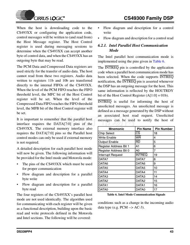
The host indicates that this is a write cycle by
driving the R/W pin low.
2) The host initiates a write cycle by driving the
CS and DS pins low.
3) The host drives the data byte to the DATA[7:0]
pins of the CS493XX.
4) Once the setup time for the write has been met,
R/W (LOW)
ADDRESS A PARALLEL I/O REGISTER
(A[1:0] SET APPROPRIATELY
C S (L O W )
D S (LO W )
WRITE BYTE TO
DATA [7:0]
Table 7. Motorola Mode Communication Signals
6.2.2.1.Writing a Byte in Motorola Mode
Information provided in this section is intended as
a functional description of how to write control
information to the CS493XX. The system designer
DS339PP4
CS (HIGH)
DS (HIGH)
Figure 26. Motorola Mode, One-Byte Write Flow
Diagram
45


 1
1
 2
2
 3
3
 4
4
 5
5
 6
6
 7
7
 8
8
 9
9
 10
10
 11
11
 12
12
 13
13
 14
14
 15
15
 16
16
 17
17
 18
18
 19
19
 20
20
 21
21
 22
22
 23
23
 24
24
 25
25
 26
26
 27
27
 28
28
 29
29
 30
30
 31
31
 32
32
 33
33
 34
34
 35
35
 36
36
 37
37
 38
38
 39
39
 40
40
 41
41
 42
42
 43
43
 44
44
 45
45
 46
46
 47
47
 48
48
 49
49
 50
50
 51
51
 52
52
 53
53
 54
54
 55
55
 56
56
 57
57
 58
58
 59
59
 60
60
 61
61
 62
62
 63
63
 64
64
 65
65
 66
66
 67
67
 68
68
 69
69
 70
70
 71
71
 72
72
 73
73
 74
74
 75
75
 76
76
 77
77
 78
78
 79
79
 80
80
 81
81
 82
82
 83
83
 84
84
 85
85
 86
86
