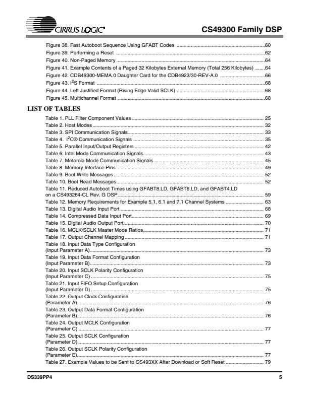
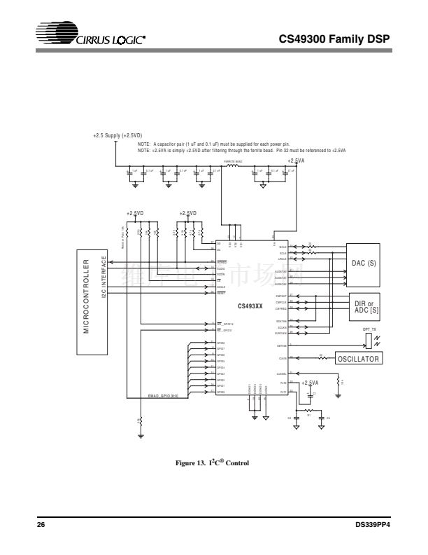
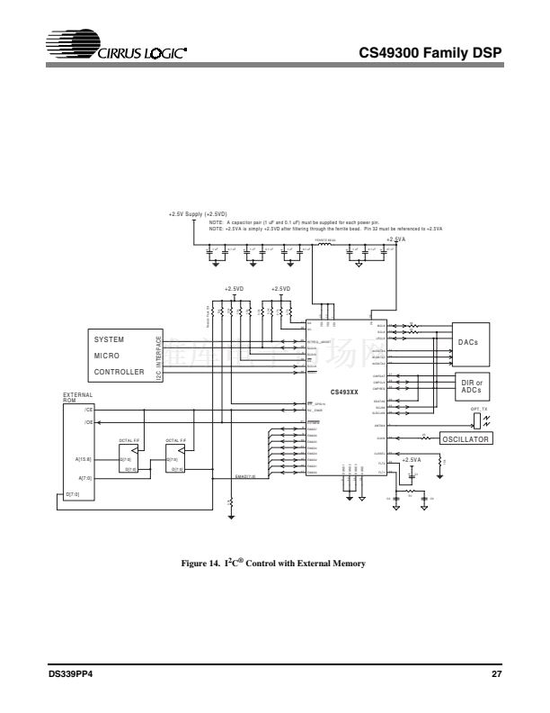
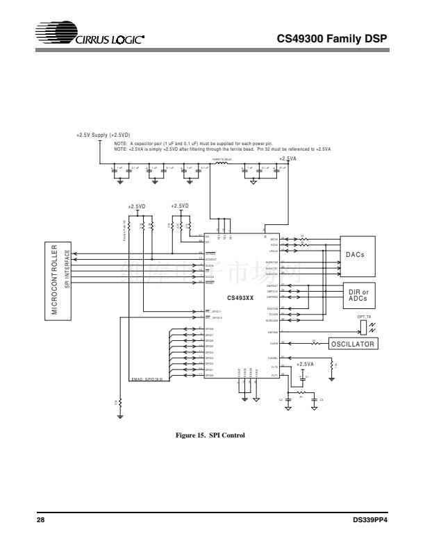
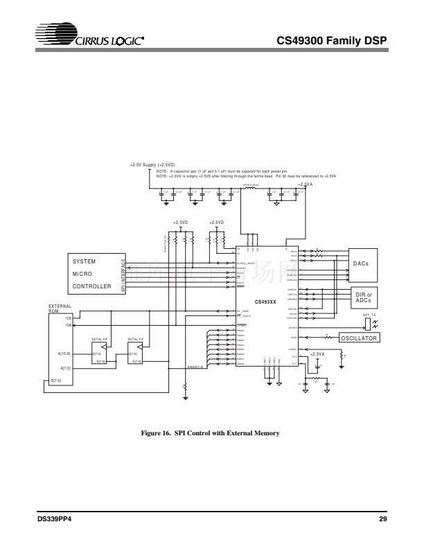
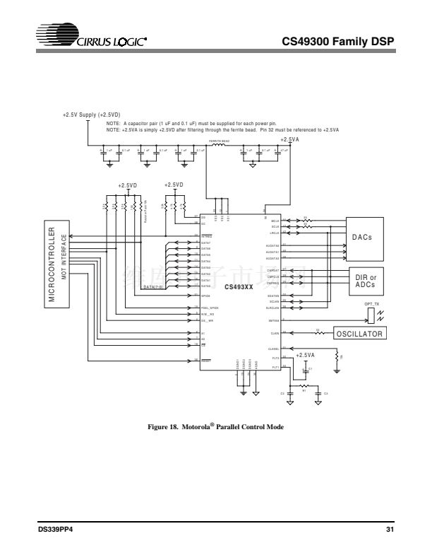
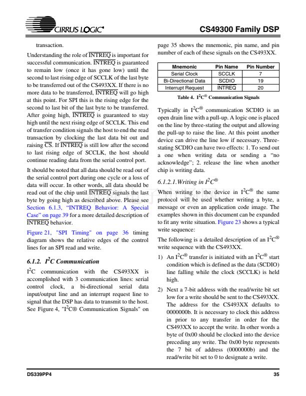
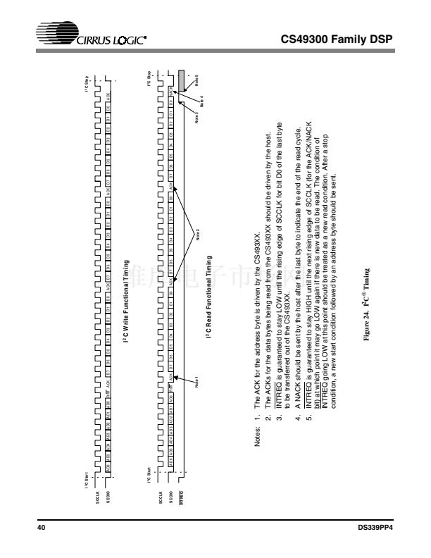
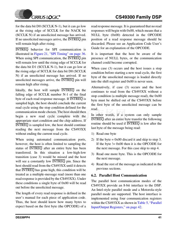
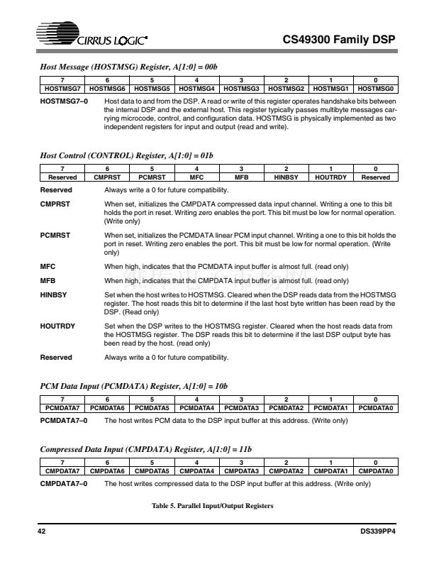
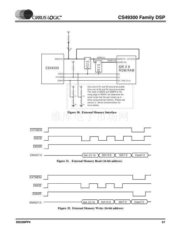
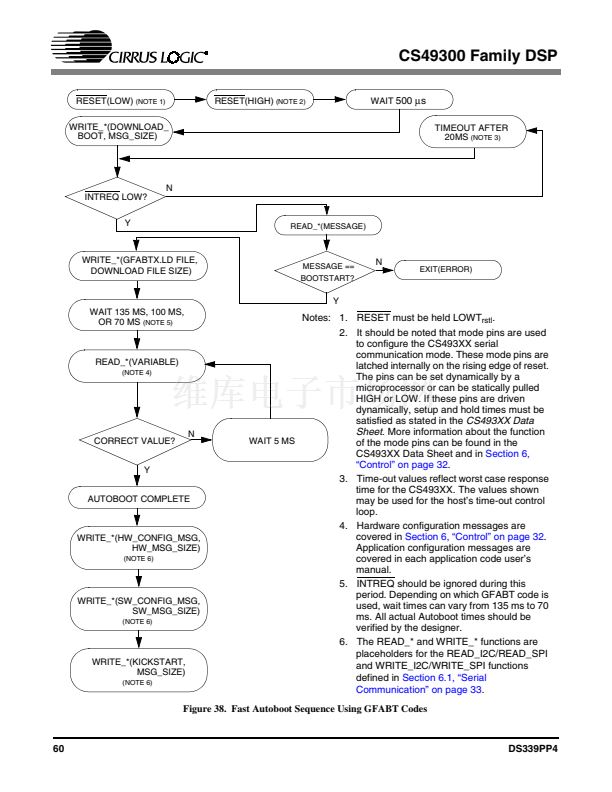
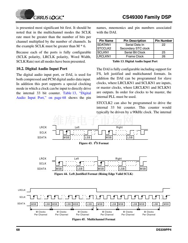
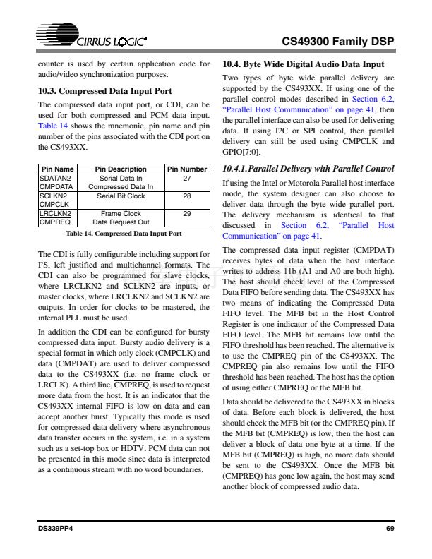
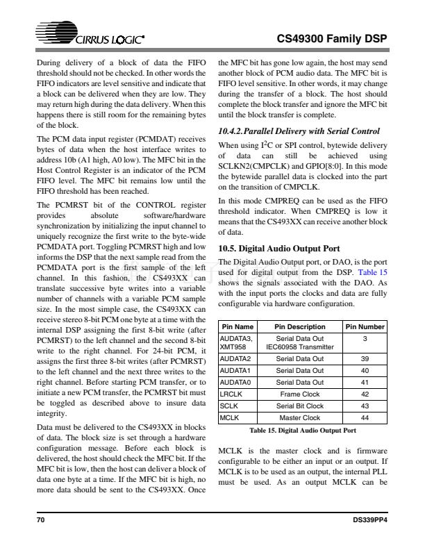
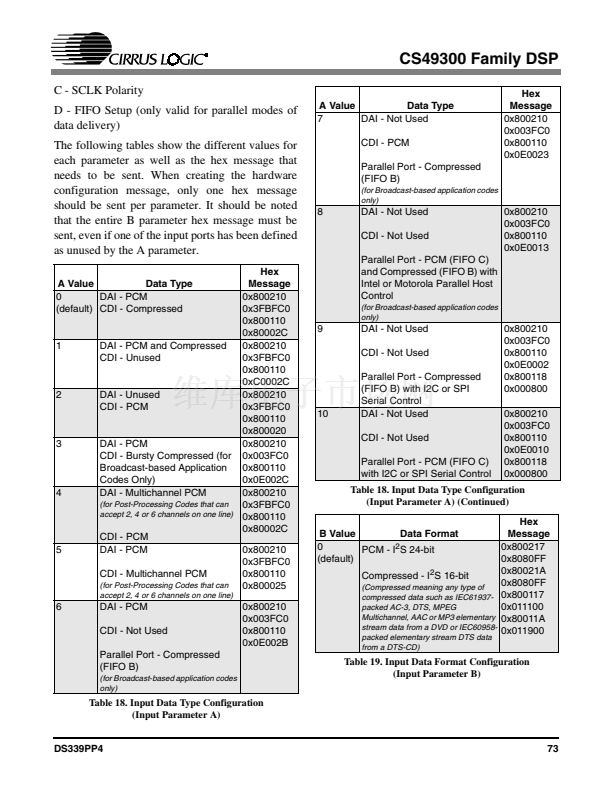
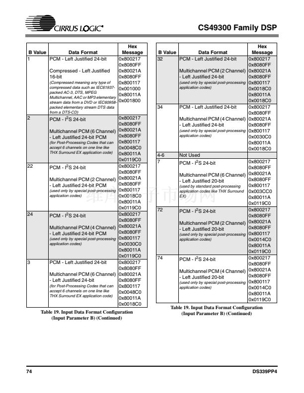
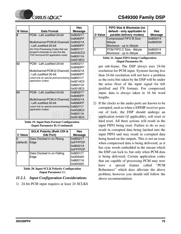
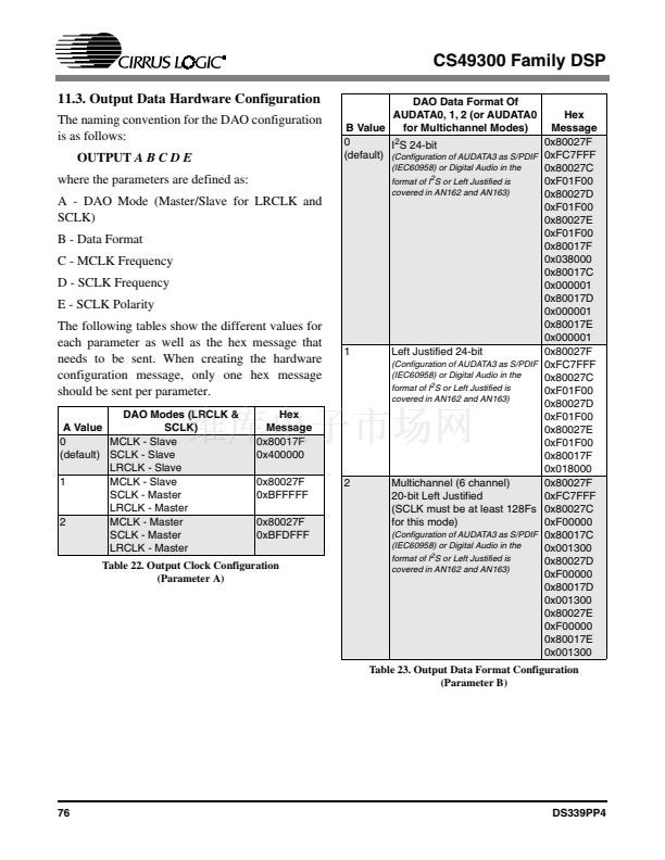
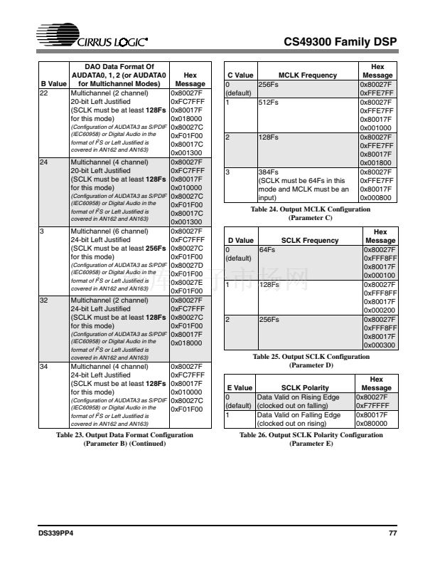
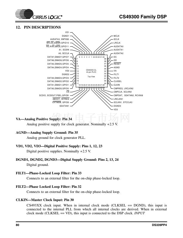
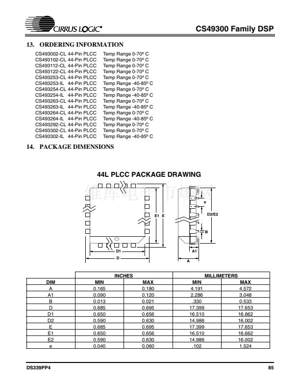
CS49300 Family DSP
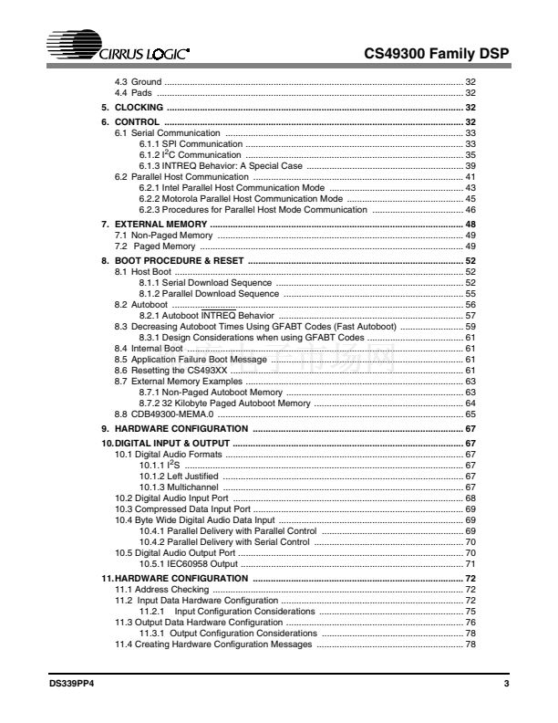
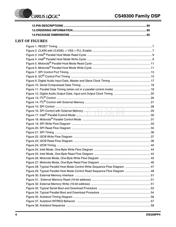
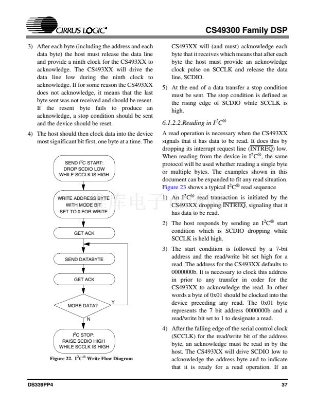
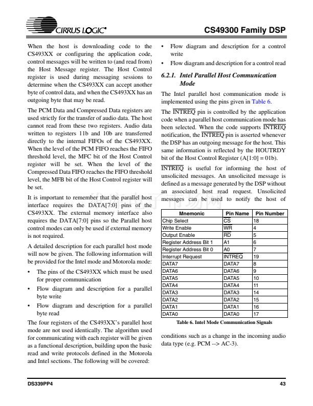
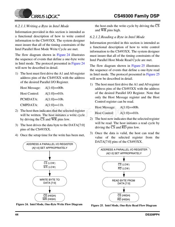
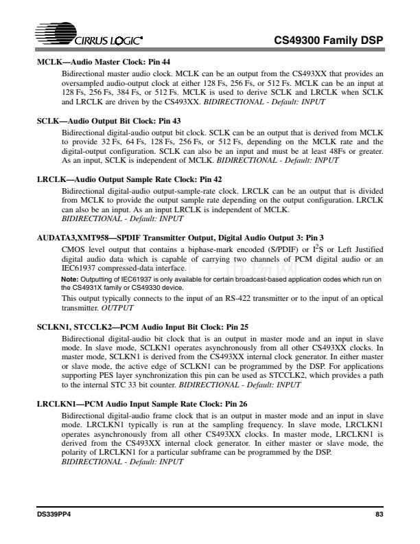
6.2.1.1.Writing a Byte in Intel Mode
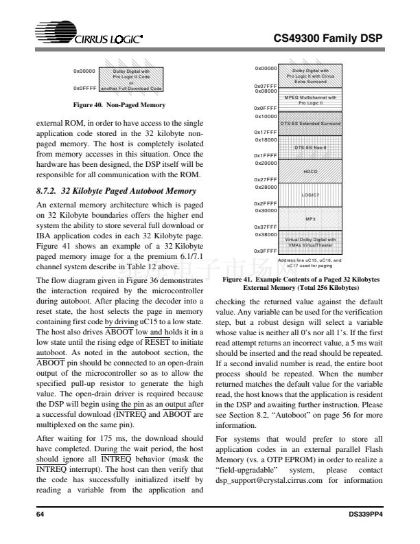
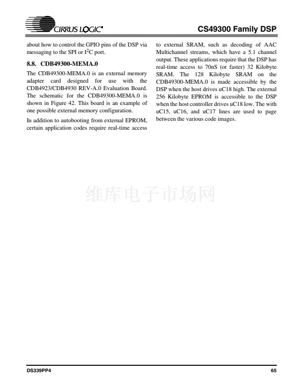
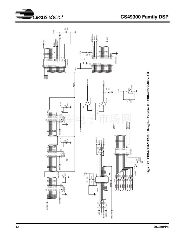
Information provided in this section is intended as
a functional description of how to write control
information to the CS493XX. The system designer
must insure that all of the timing constraints of the
Intel Parallel Host Mode Write Cycle are met.
The flow diagram shown in
Figure 24
illustrates
the sequence of events that define a one-byte write
in Intel mode. The protocol presented in
Figure 24
will now be described in detail.
1) The host must first drive the A1 and A0 register
address pins of the CS493XX with the address
of the desired Parallel I/O Register.
Host Message:
Host Control:
PCMDATA:
CMPDATA:
A[1:0]==00b.
A[1:0]==01b.
A[1:0]==10b.
A[1:0]==11b.
the host ends the write cycle by driving the CS
and WR pins high.
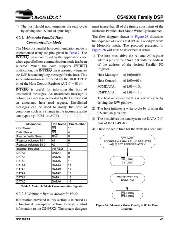
6.2.1.2.Reading a Byte in Intel Mode
Information provided in this section is intended as
a functional description of how to write control
information to the CS493XX. The system designer
must insure that all of the timing constraints of the
Intel Parallel Host Mode Read Cycle are met.
The flow diagram shown in
Figure 25
illustrates
the sequence of events that define a one-byte read
in Intel mode. The protocol presented in
Figure 25
will now be described in detail.
1) The host must first drive the A1 and A0 register
address pins of the CS493XX with the address
of the desired Parallel I/O Register. Note that
only the Host Message register and the Host
Control register can be read.
Host Message:
Host Control:
A[1:0]==00b.
A[1:0]==01b.
2) The host then indicates that the selected register
will be written. The host initiates a write cycle
by driving the CS and WR pins low.
3) The host drives the data byte to the DATA[7:0]
pins of the CS493XX.
4) Once the setup time for the write has been met,
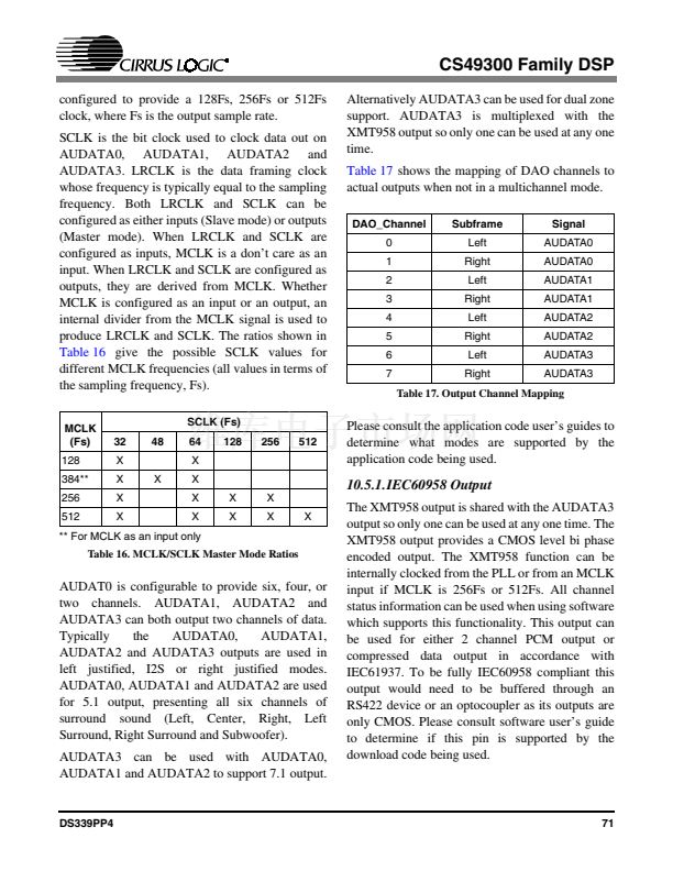
ADDRESS A PARALLEL I/O REGISTER
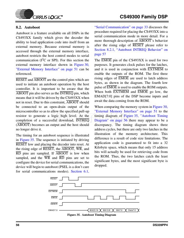
(A[1:0] SET APPROPRIATELY
2) The host now indicates that the selected register
will be read. The host initiates a read cycle by
driving the CS and RD pins low.
3) Once the data is valid, the host can read the
value of the selected register from the
DATA[7:0] pins of the CS493XX.
ADDRESS A PARALLEL I/O REGISTER
(A[1:0] SET APPROPRIATELY
C S (LO W )
W R (LO W )
C S (LO W )
R D (LO W )
WRITE BYTE TO
DATA [7:0]
READ BYTE FROM
DATA [7:0]
CS (HIGH)
WR (HIGH)
CS (HIGH)
RD (HIGH)
Figure 24. Intel Mode, One-Byte Write Flow Diagram
Figure 25. Intel Mode, One-Byte Read Flow Diagram
DS339PP4
44


 1
1
 2
2
 3
3
 4
4
 5
5
 6
6
 7
7
 8
8
 9
9
 10
10
 11
11
 12
12
 13
13
 14
14
 15
15
 16
16
 17
17
 18
18
 19
19
 20
20
 21
21
 22
22
 23
23
 24
24
 25
25
 26
26
 27
27
 28
28
 29
29
 30
30
 31
31
 32
32
 33
33
 34
34
 35
35
 36
36
 37
37
 38
38
 39
39
 40
40
 41
41
 42
42
 43
43
 44
44
 45
45
 46
46
 47
47
 48
48
 49
49
 50
50
 51
51
 52
52
 53
53
 54
54
 55
55
 56
56
 57
57
 58
58
 59
59
 60
60
 61
61
 62
62
 63
63
 64
64
 65
65
 66
66
 67
67
 68
68
 69
69
 70
70
 71
71
 72
72
 73
73
 74
74
 75
75
 76
76
 77
77
 78
78
 79
79
 80
80
 81
81
 82
82
 83
83
 84
84
 85
85
 86
86
