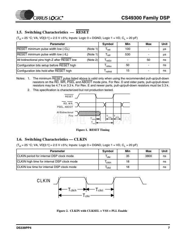
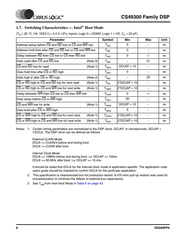
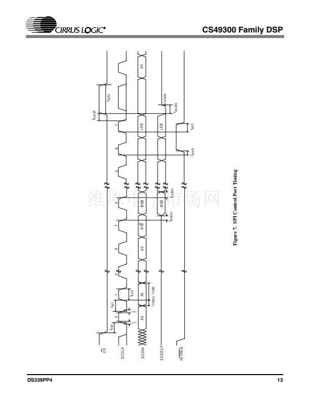
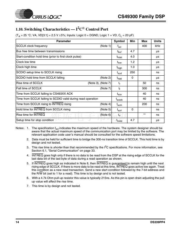
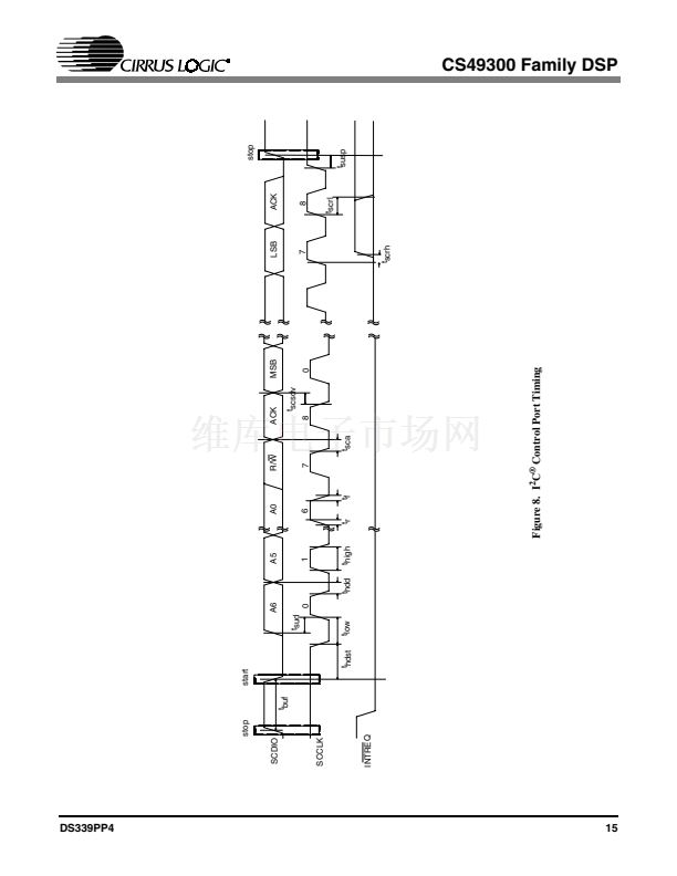
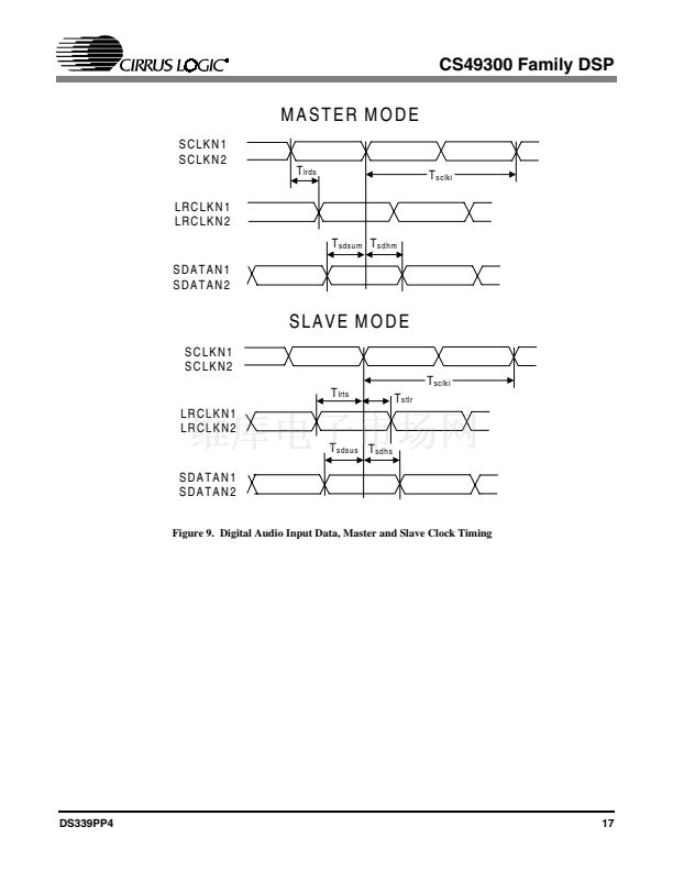
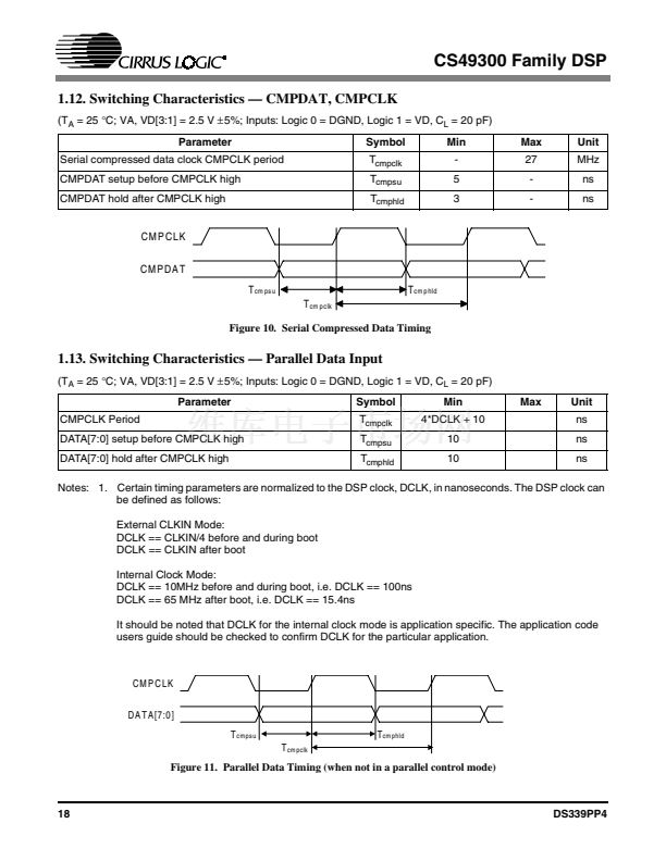
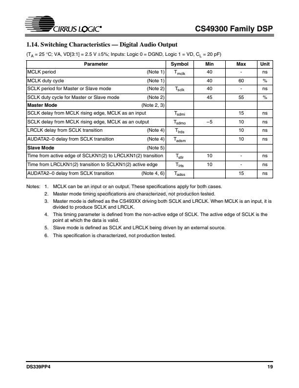
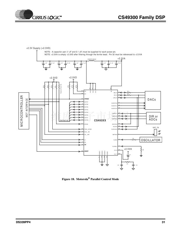
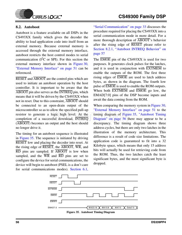
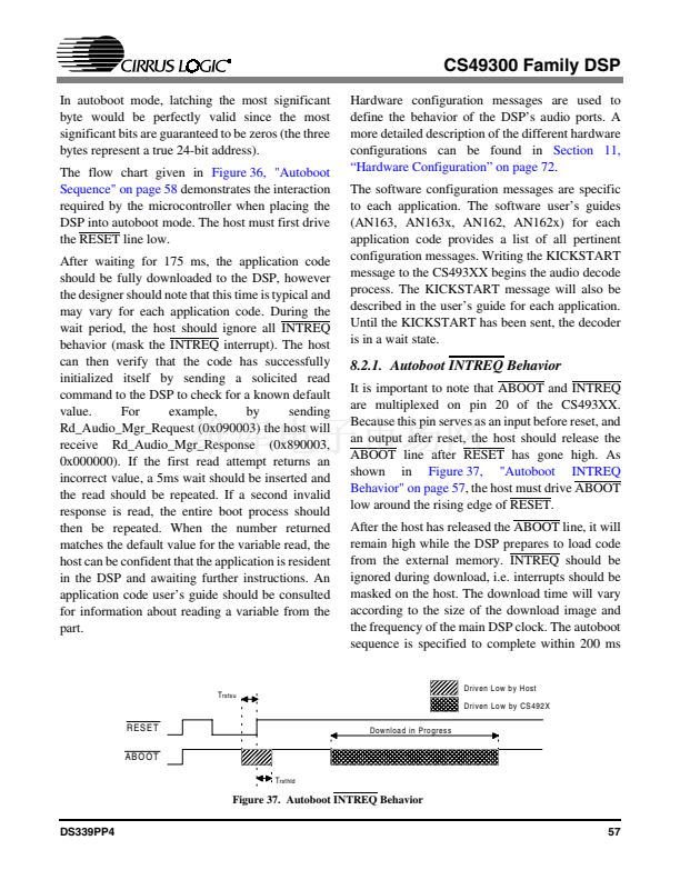
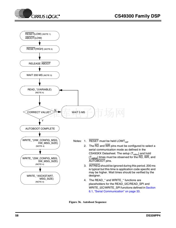
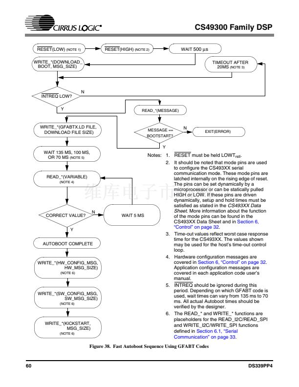
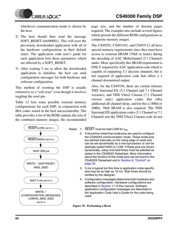
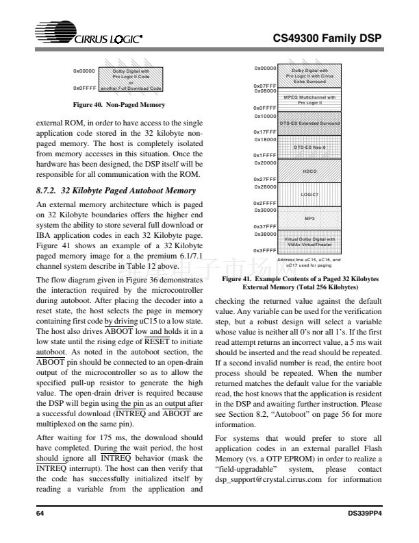
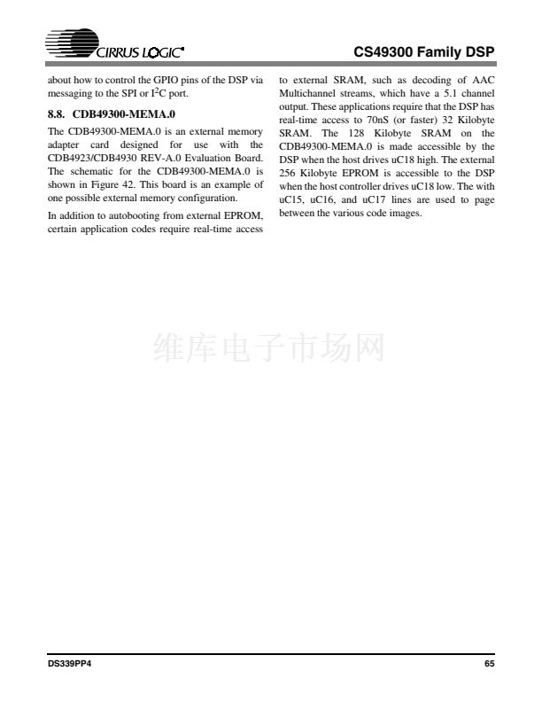
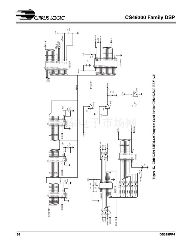
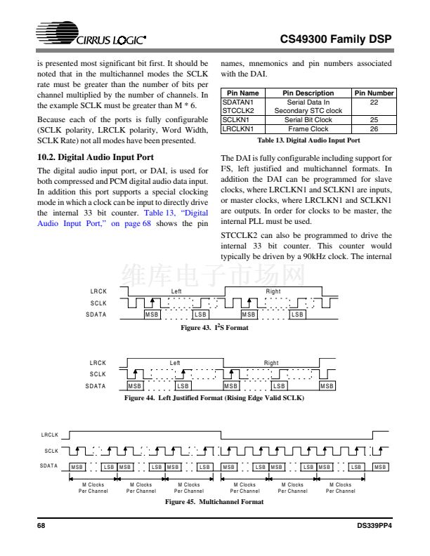
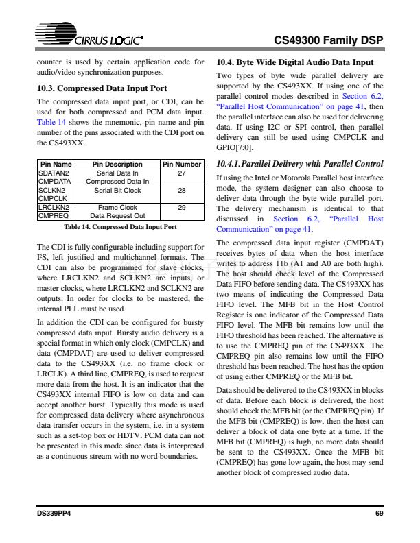
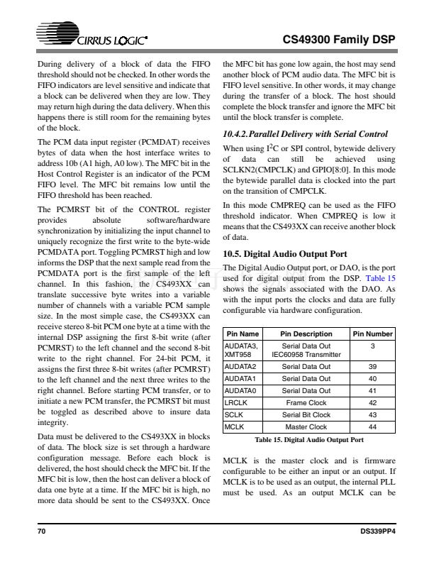
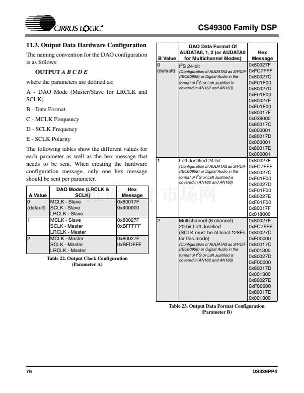
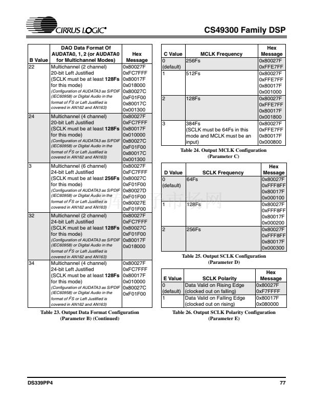
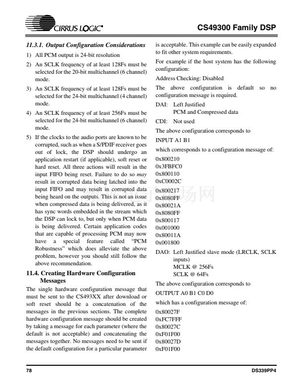
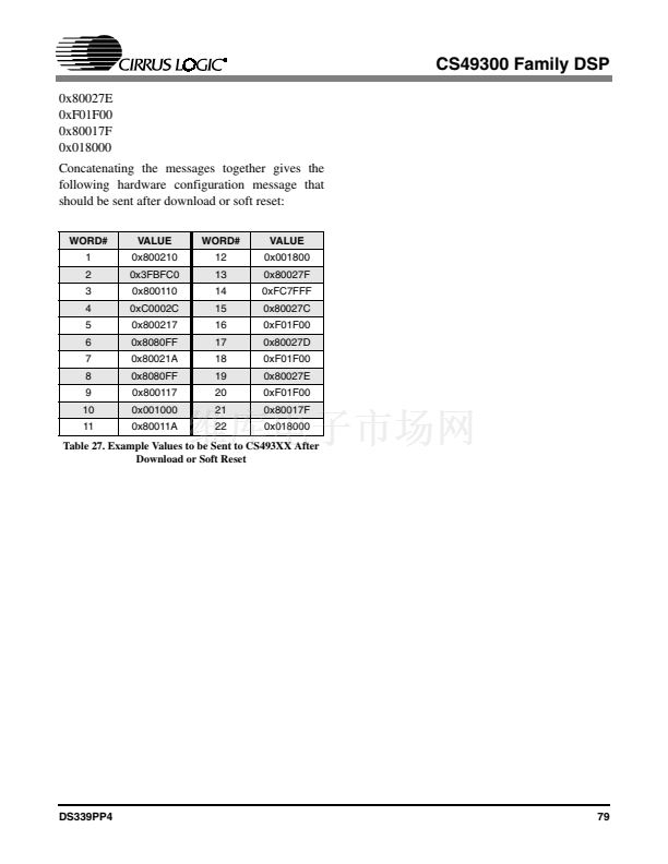
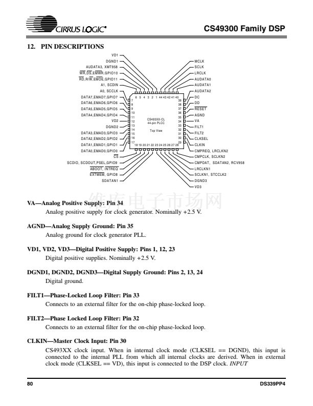
CS49300 Family DSP
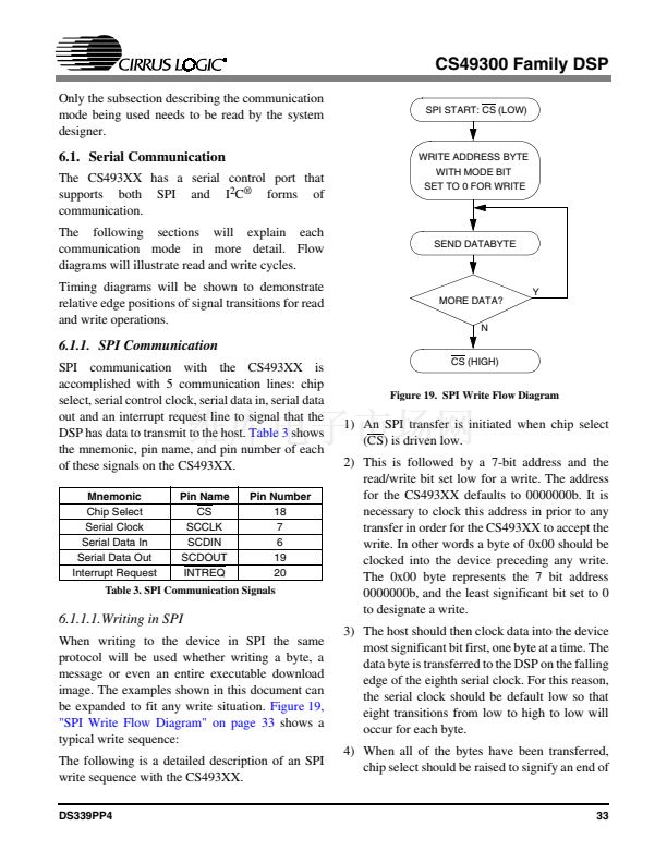
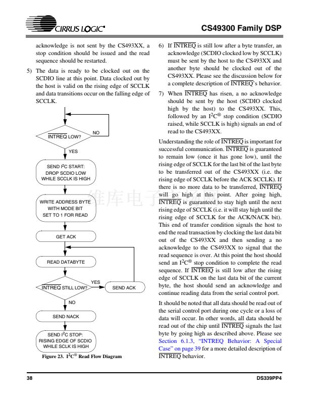
write. Once again it is crucial that the serial
clock transitions from high to low on the last bit
of the last byte before chip select is raised, or a
loss of data will occur.
The same write routine could be used to send a
single byte, message or an entire application code
image. From a hardware perspective, it makes no
difference whether communication is by byte or
multiple bytes of any length as long as the correct
hardware protocol is followed.
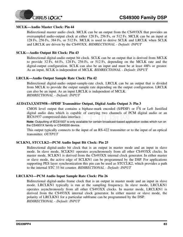
INTREQ
LOW?
YES
CS (LOW)
NO
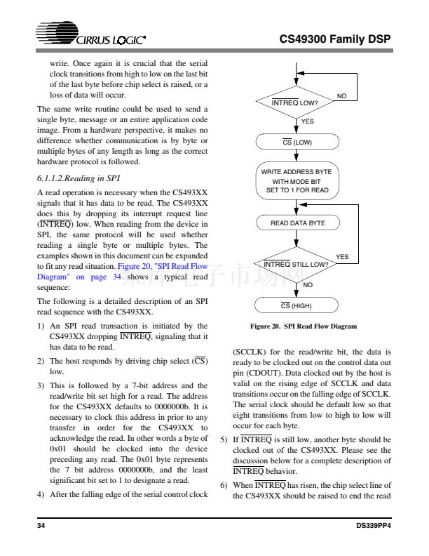
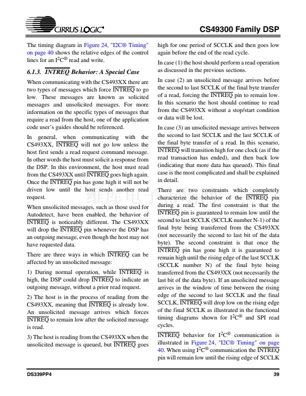
6.1.1.2.Reading in SPI
A read operation is necessary when the CS493XX
signals that it has data to be read. The CS493XX
does this by dropping its interrupt request line
(INTREQ) low. When reading from the device in
SPI, the same protocol will be used whether
reading a single byte or multiple bytes. The
examples shown in this document can be expanded
to fit any read situation.
Figure 20, "SPI Read Flow
Diagram" on page 34
shows a typical read
sequence:
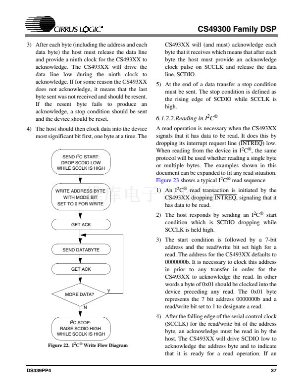
The following is a detailed description of an SPI
read sequence with the CS493XX.
1) An SPI read transaction is initiated by the
CS493XX dropping INTREQ, signaling that it
has data to be read.
2) The host responds by driving chip select (CS)
low.
3) This is followed by a 7-bit address and the
read/write bit set high for a read. The address
for the CS493XX defaults to 0000000b. It is
necessary to clock this address in prior to any
transfer in order for the CS493XX to
acknowledge the read. In other words a byte of
0x01 should be clocked into the device
preceding any read. The 0x01 byte represents
the 7 bit address 0000000b, and the least
significant bit set to 1 to designate a read.
4) After the falling edge of the serial control clock
WRITE ADDRESS BYTE
WITH MODE BIT
SET TO 1 FOR READ
READ DATA BYTE
YES
INTREQ
STILL LOW?
NO
CS (HIGH)
Figure 20. SPI Read Flow Diagram
(SCCLK) for the read/write bit, the data is
ready to be clocked out on the control data out
pin (CDOUT). Data clocked out by the host is
valid on the rising edge of SCCLK and data
transitions occur on the falling edge of SCCLK.
The serial clock should be default low so that
eight transitions from low to high to low will
occur for each byte.
5) If INTREQ is still low, another byte should be
clocked out of the CS493XX. Please see the
discussion below for a complete description of
INTREQ behavior.
6) When INTREQ has risen, the chip select line of
the CS493XX should be raised to end the read
34
DS339PP4


 1
1
 2
2
 3
3
 4
4
 5
5
 6
6
 7
7
 8
8
 9
9
 10
10
 11
11
 12
12
 13
13
 14
14
 15
15
 16
16
 17
17
 18
18
 19
19
 20
20
 21
21
 22
22
 23
23
 24
24
 25
25
 26
26
 27
27
 28
28
 29
29
 30
30
 31
31
 32
32
 33
33
 34
34
 35
35
 36
36
 37
37
 38
38
 39
39
 40
40
 41
41
 42
42
 43
43
 44
44
 45
45
 46
46
 47
47
 48
48
 49
49
 50
50
 51
51
 52
52
 53
53
 54
54
 55
55
 56
56
 57
57
 58
58
 59
59
 60
60
 61
61
 62
62
 63
63
 64
64
 65
65
 66
66
 67
67
 68
68
 69
69
 70
70
 71
71
 72
72
 73
73
 74
74
 75
75
 76
76
 77
77
 78
78
 79
79
 80
80
 81
81
 82
82
 83
83
 84
84
 85
85
 86
86
