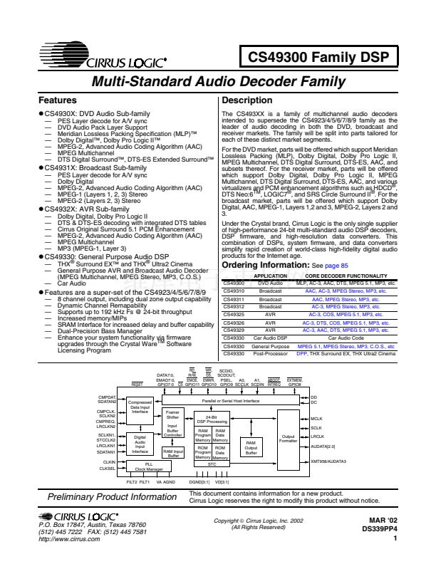
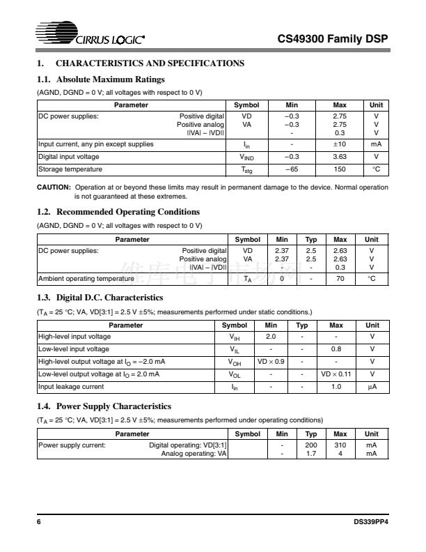
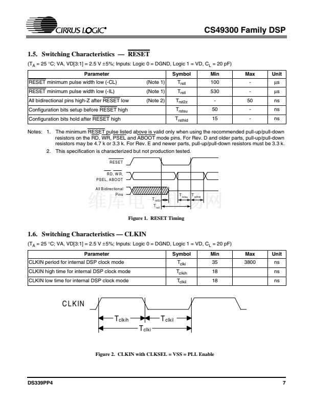
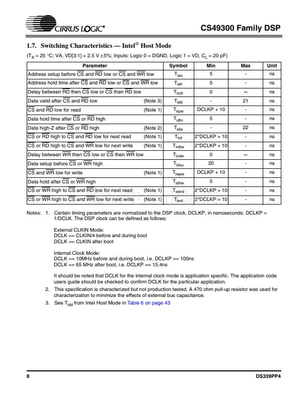
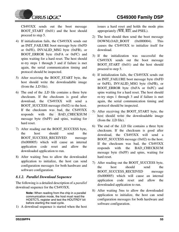
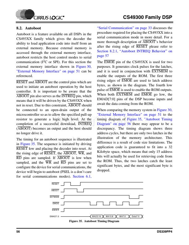
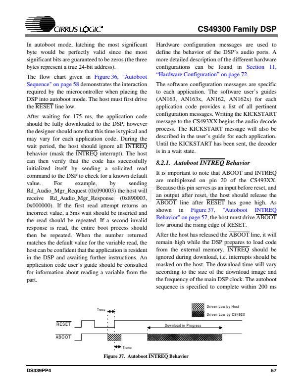
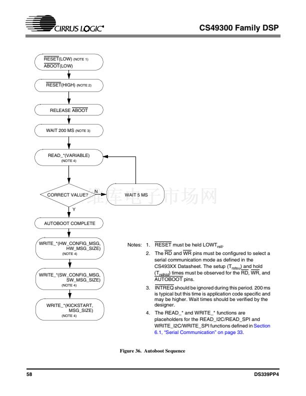
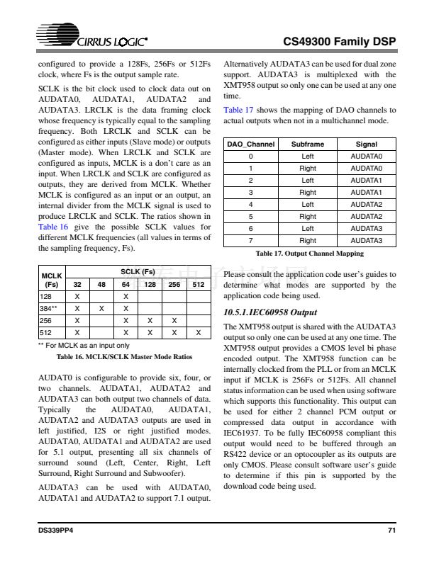
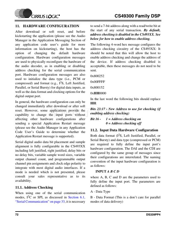
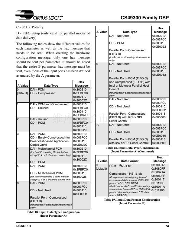
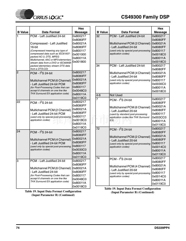
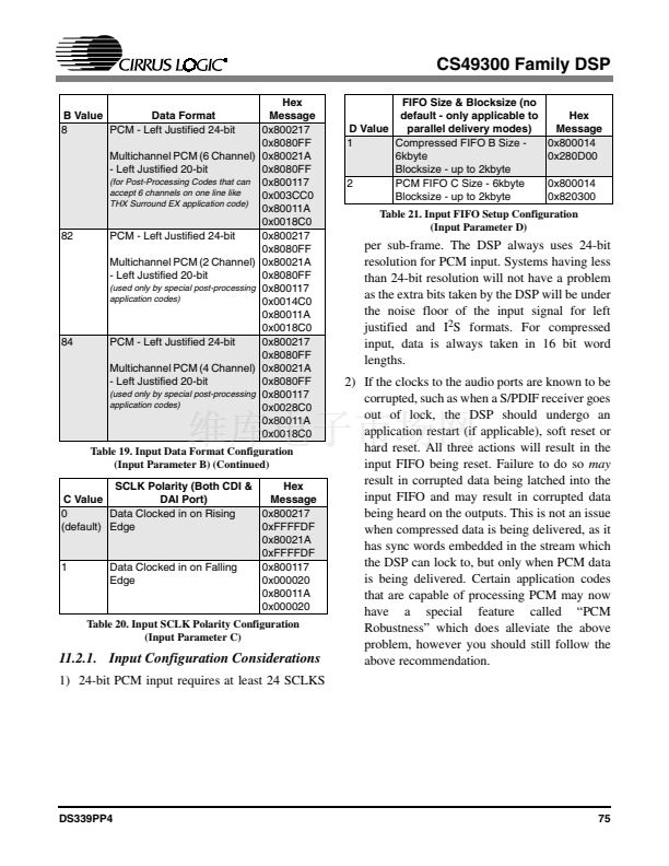
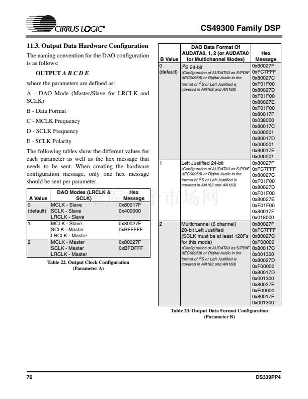
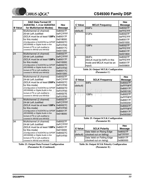
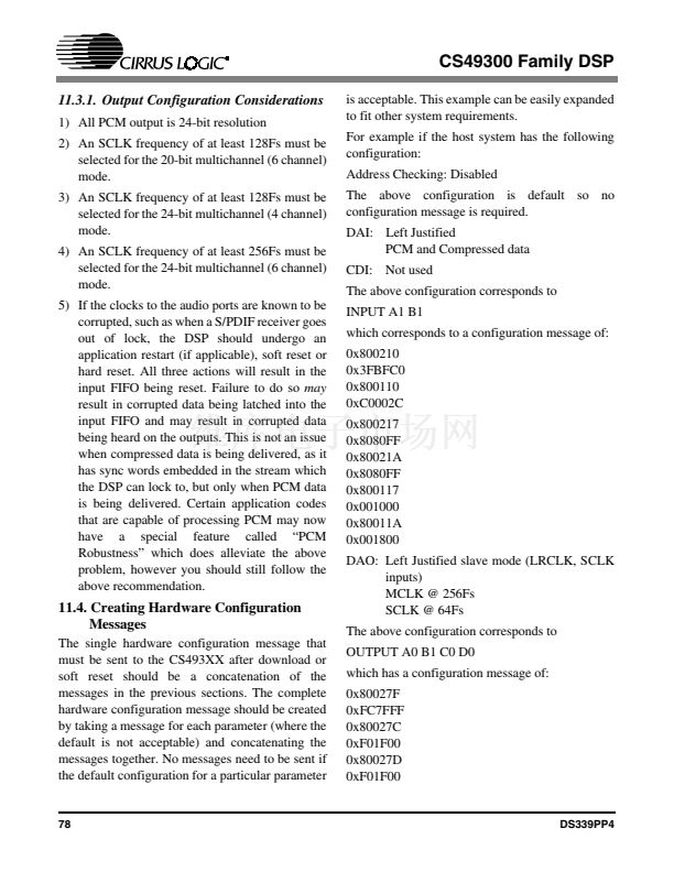
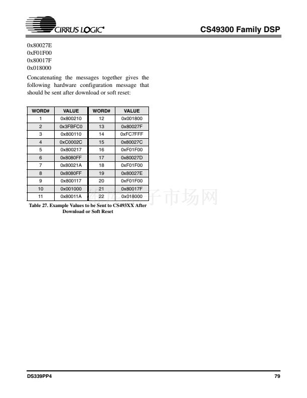
CS49300 Family DSP
Only the subsection describing the communication
mode being used needs to be read by the system
designer.
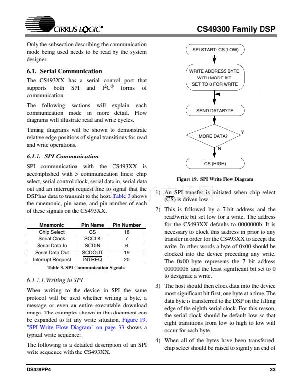
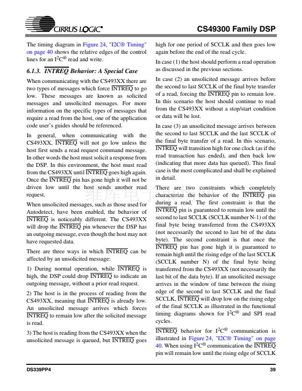
SPI START: CS (LOW)
6.1. Serial Communication
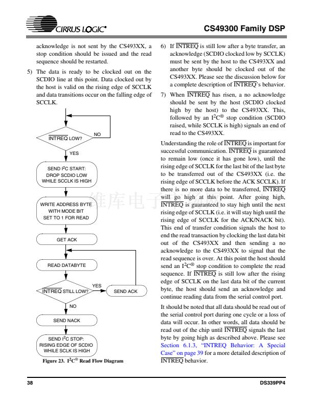
The CS493XX has a serial control port that
supports both SPI and I
2
C
廬
forms of
communication.
The following sections will explain each
communication mode in more detail. Flow
diagrams will illustrate read and write cycles.
Timing diagrams will be shown to demonstrate
relative edge positions of signal transitions for read
and write operations.
WRITE ADDRESS BYTE
WITH MODE BIT
SET TO 0 FOR WRITE
SEND DATABYTE
Y
MORE DATA?
N
6.1.1. SPI Communication
SPI communication with the CS493XX is
accomplished with 5 communication lines: chip
select, serial control clock, serial data in, serial data
out and an interrupt request line to signal that the
DSP has data to transmit to the host.
Table 3
shows
the mnemonic, pin name, and pin number of each
of these signals on the CS493XX.
Mnemonic
Chip Select
Serial Clock
Serial Data In
Serial Data Out
Interrupt Request
Pin Name
CS
SCCLK
SCDIN
SCDOUT
INTREQ
Pin Number
18
7
6
19
20
CS (HIGH)
Figure 19. SPI Write Flow Diagram
1) An SPI transfer is initiated when chip select
(CS) is driven low.
2) This is followed by a 7-bit address and the
read/write bit set low for a write. The address
for the CS493XX defaults to 0000000b. It is
necessary to clock this address in prior to any
transfer in order for the CS493XX to accept the
write. In other words a byte of 0x00 should be
clocked into the device preceding any write.
The 0x00 byte represents the 7 bit address
0000000b, and the least significant bit set to 0
to designate a write.
3) The host should then clock data into the device
most significant bit first, one byte at a time. The
data byte is transferred to the DSP on the falling
edge of the eighth serial clock. For this reason,
the serial clock should be default low so that
eight transitions from low to high to low will
occur for each byte.
4) When all of the bytes have been transferred,
chip select should be raised to signify an end of
Table 3. SPI Communication Signals
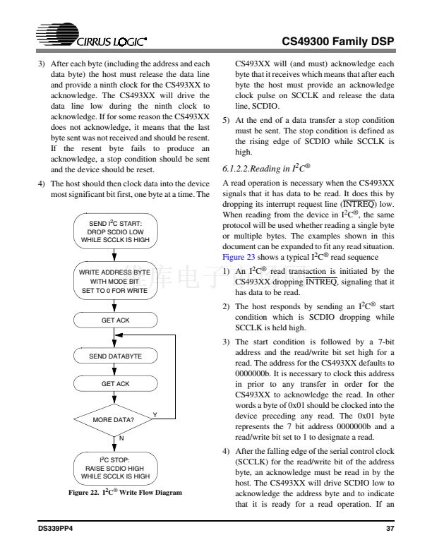
6.1.1.1.Writing in SPI
When writing to the device in SPI the same
protocol will be used whether writing a byte, a
message or even an entire executable download
image. The examples shown in this document can
be expanded to fit any write situation.
Figure 19,
"SPI Write Flow Diagram" on page 33
shows a
typical write sequence:
The following is a detailed description of an SPI
write sequence with the CS493XX.
DS339PP4
33


 1
1
 2
2
 3
3
 4
4
 5
5
 6
6
 7
7
 8
8
 9
9
 10
10
 11
11
 12
12
 13
13
 14
14
 15
15
 16
16
 17
17
 18
18
 19
19
 20
20
 21
21
 22
22
 23
23
 24
24
 25
25
 26
26
 27
27
 28
28
 29
29
 30
30
 31
31
 32
32
 33
33
 34
34
 35
35
 36
36
 37
37
 38
38
 39
39
 40
40
 41
41
 42
42
 43
43
 44
44
 45
45
 46
46
 47
47
 48
48
 49
49
 50
50
 51
51
 52
52
 53
53
 54
54
 55
55
 56
56
 57
57
 58
58
 59
59
 60
60
 61
61
 62
62
 63
63
 64
64
 65
65
 66
66
 67
67
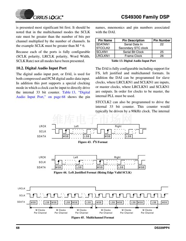 68
68
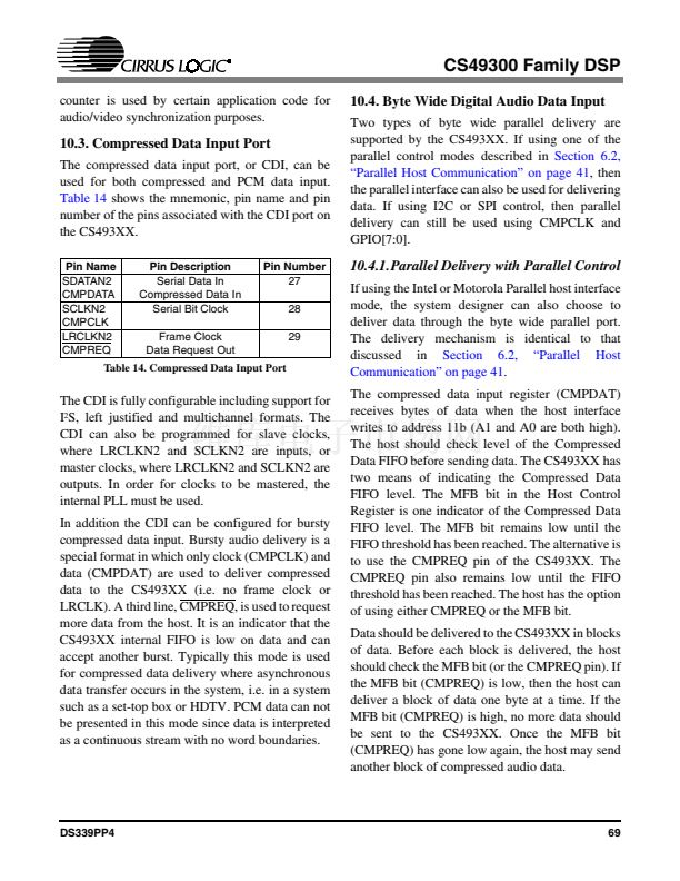 69
69
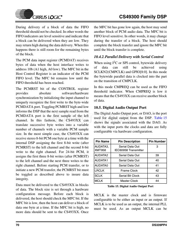 70
70
 71
71
 72
72
 73
73
 74
74
 75
75
 76
76
 77
77
 78
78
 79
79
 80
80
 81
81
 82
82
 83
83
 84
84
 85
85
 86
86
