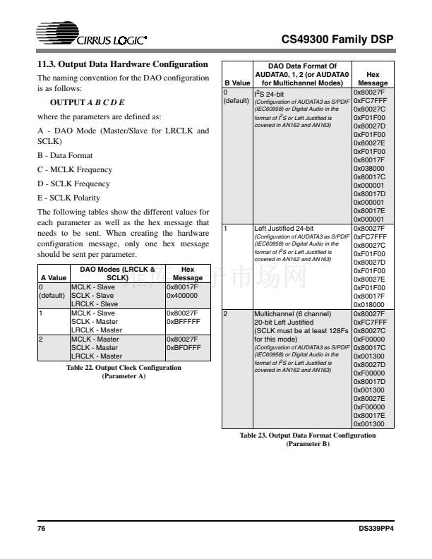
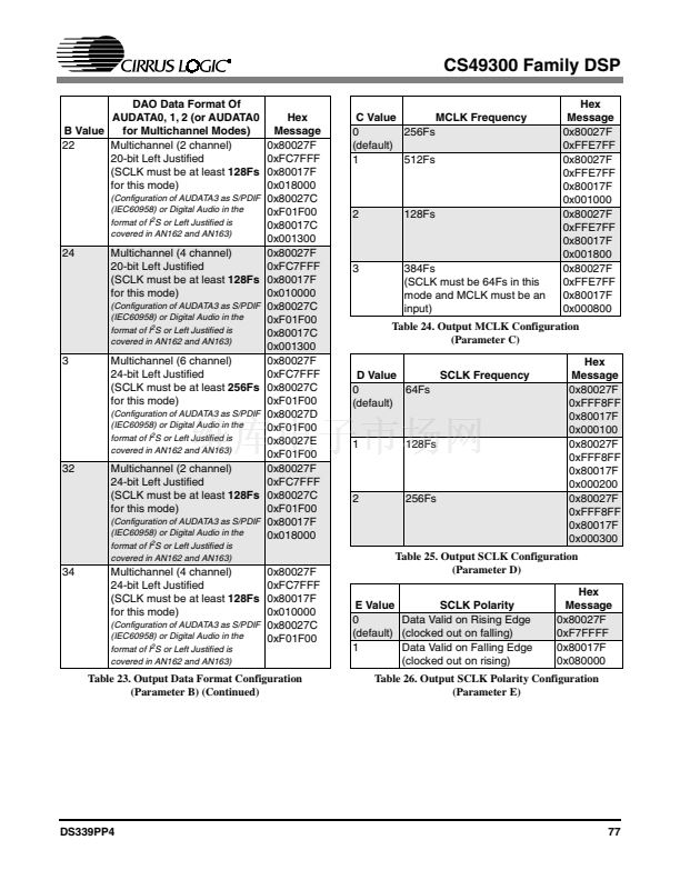
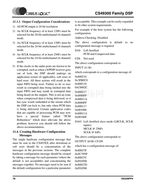
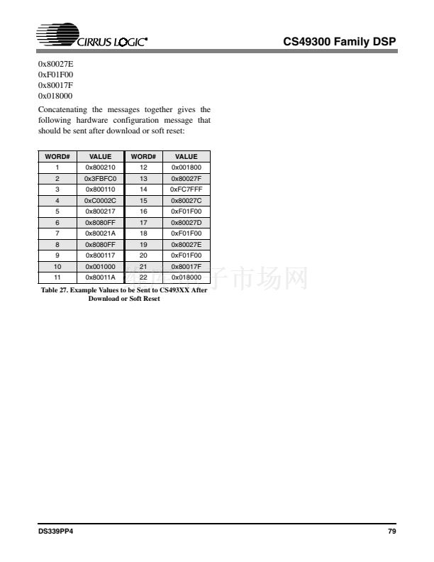
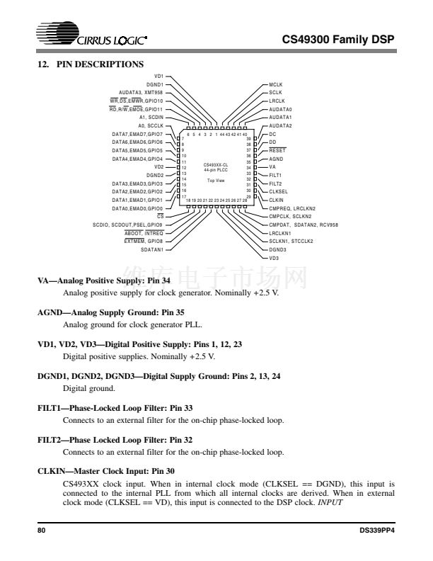
CS49300 Family DSP
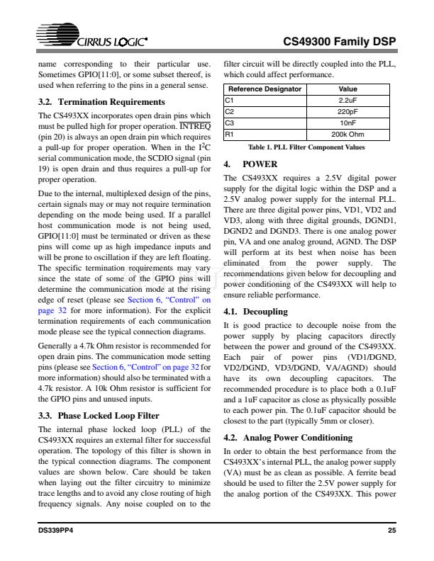
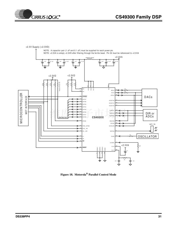
scheme is shown in the typical connection
diagrams.
even multiples of the desired sampling rate or with
an already available clock source. Typically a
12.288 MHz CLKIN is used in this scenario so that
the same oscillator can be used for the DSP and
ADC.
The clock manager is controlled by the DSP
application software. The software user鈥檚 guide for
the application code being used should be
referenced for what CLKIN input frequency is
supported.
4.3. Ground
For two layer applications, care should be taken to
have sufficient ground between the DSP and parts
in which it will be interfacing (DACs, ADCs, DIR,
microcontrollers, external memory etc). If there is
not sufficient ground, a potential will be seen
between the ground reference of the DSP and the
interface parts and the noise margin will be
significantly
reduced
potentially
causing
communication or data integrity problems.
6.
CONTROL
4.4. Pads
The CS493XX incorporate 3.3V tolerant pads. This
means that while the CS493XX power supplies
require 2.5 volts, 3.3 volt signals can be applied to
the inputs without damaging the part.
5.
CLOCKING
The CS493XX clock manager incorporates a
programmable phase locked loop (PLL) clock
synthesizer. The PLL takes an input reference
clock and produces all the internal clocks required
to run the internal DSP and to provide master mode
timing to the audio input/output peripherals. The
clock manager also includes a 33-bit system time
clock (STC) to support audio and video
synchronization.
The PLL can be internally bypassed by connecting
the CLKSEL pin to VD. This connection
multiplexes the CLKIN pin directly to the DSP
clock. Care should be taken to note the minimum
CLKIN requirements when bypassing the PLL.
The PLL reference clock has three possible sources
that are routed through a multiplexer controlled by
the DSP: SCLKN2, SCLKN1, and CLKIN.
Typically, in audio/video environments like set-top
boxes, the CLKIN pin is connected to 27 MHz. In
other scenarios such as an A/V receiver design, the
PLL can be clocked through the CLKIN pin with
32
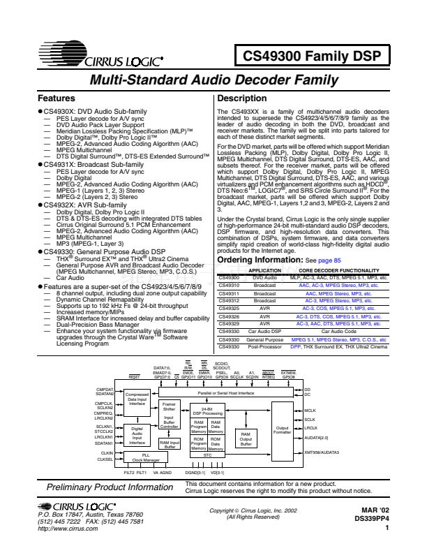
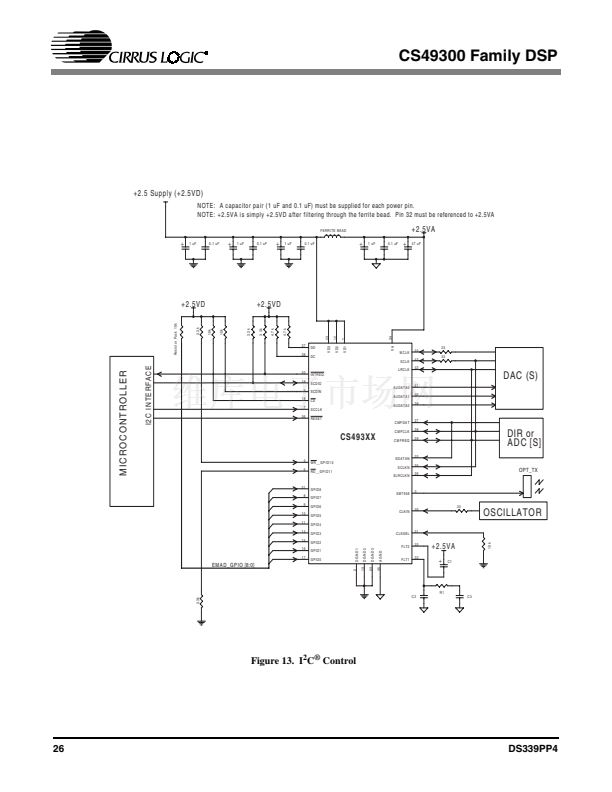
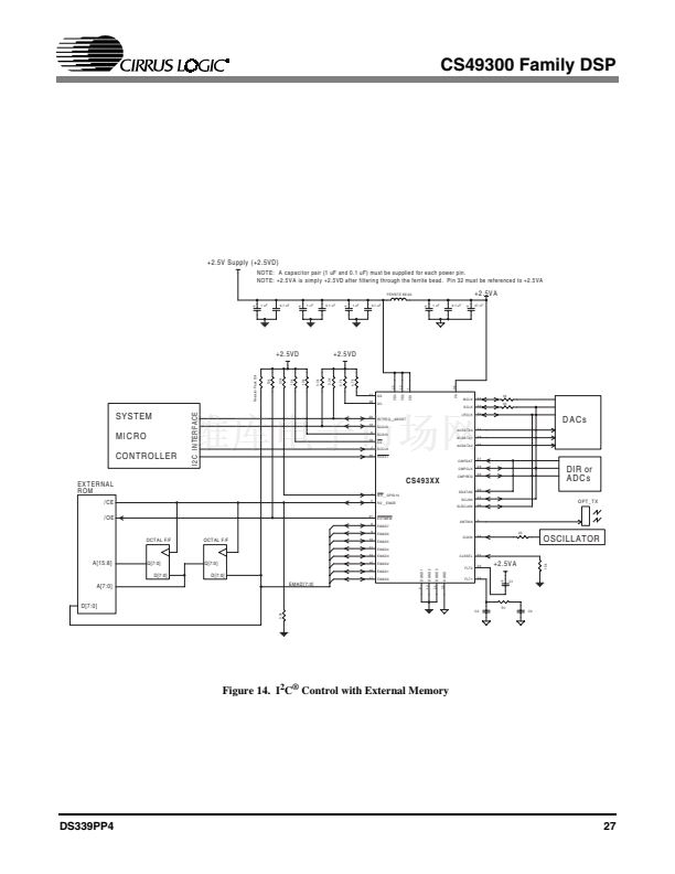
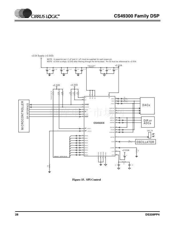
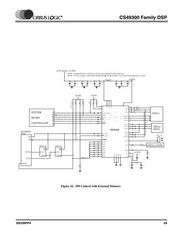
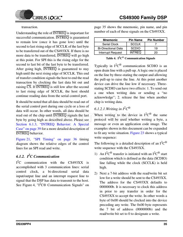
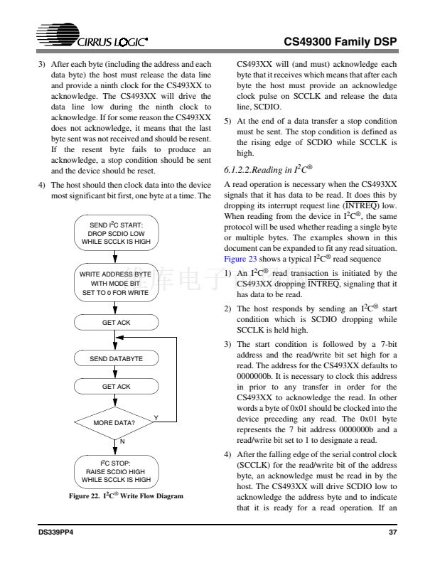
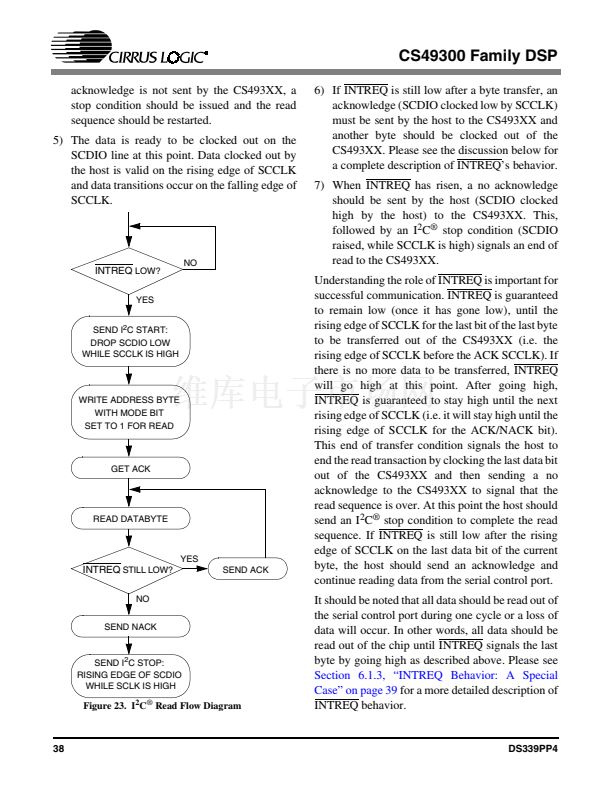
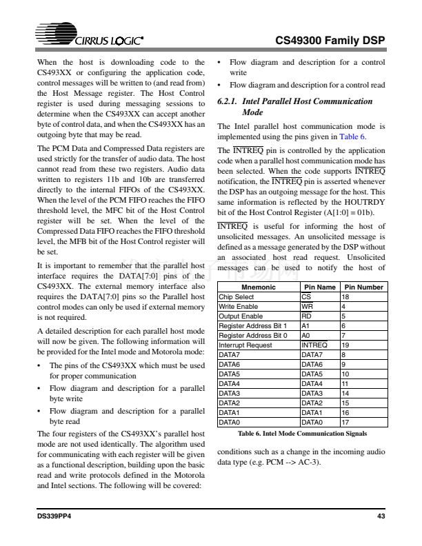
Control of the CS493XX can be accomplished
through one of four methods. The CS493XX
supports I
2
C
廬
and SPI serial communication. In
addition the CS493XX supports both a Motorola
and Intel byte wide parallel host control mode.
Only one of the four communication modes can be
selected for control. The states of the RD, WR, and
PSEL pins are sampled at the rising edge of RESET
to determine the interface type as shown in
Table 2.
RD
(Pin 5)
1
1
0
1
WR
(Pin 4)
1
1
1
0
PSEL
(Pin 19)
1
0
X
X
Table 2. Host Modes
Host Interface Mode
8-bit Motorola
廬
8-bit Intel
廬
Serial I
2
C
廬
Serial SPI
Whichever host communication mode is used, host
control of the CS493XX is handled through the
application software running on the DSP.
Configuration and control of the CS493XX
decoder and its peripherals are indirectly executed
through a messaging protocol supported by the
downloaded application code. In other words
successful communication can only be
accomplished by following the low level hardware
communication format and high level messaging
protocol. The specifications of the messaging
protocol can be found in any of the software user鈥檚
guides.
DS339PP4


 1
1
 2
2
 3
3
 4
4
 5
5
 6
6
 7
7
 8
8
 9
9
 10
10
 11
11
 12
12
 13
13
 14
14
 15
15
 16
16
 17
17
 18
18
 19
19
 20
20
 21
21
 22
22
 23
23
 24
24
 25
25
 26
26
 27
27
 28
28
 29
29
 30
30
 31
31
 32
32
 33
33
 34
34
 35
35
 36
36
 37
37
 38
38
 39
39
 40
40
 41
41
 42
42
 43
43
 44
44
 45
45
 46
46
 47
47
 48
48
 49
49
 50
50
 51
51
 52
52
 53
53
 54
54
 55
55
 56
56
 57
57
 58
58
 59
59
 60
60
 61
61
 62
62
 63
63
 64
64
 65
65
 66
66
 67
67
 68
68
 69
69
 70
70
 71
71
 72
72
 73
73
 74
74
 75
75
 76
76
 77
77
 78
78
 79
79
 80
80
 81
81
 82
82
 83
83
 84
84
 85
85
 86
86
