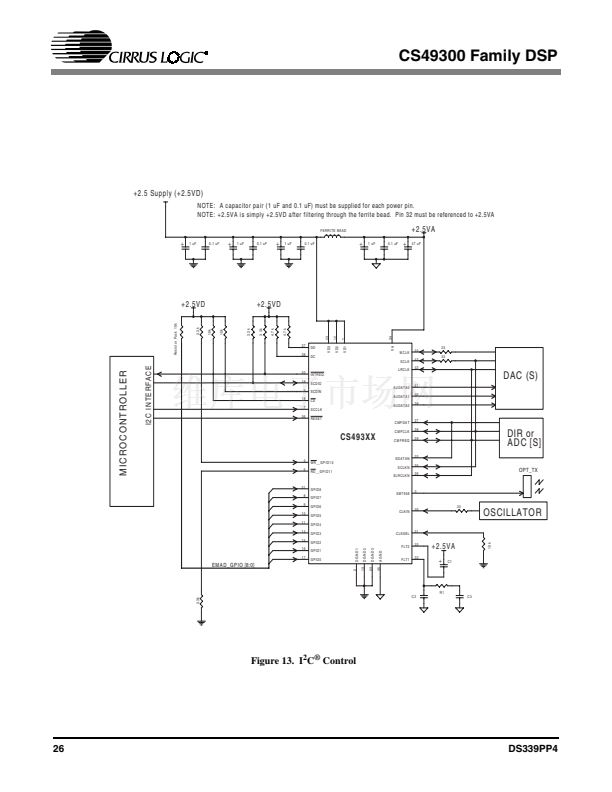
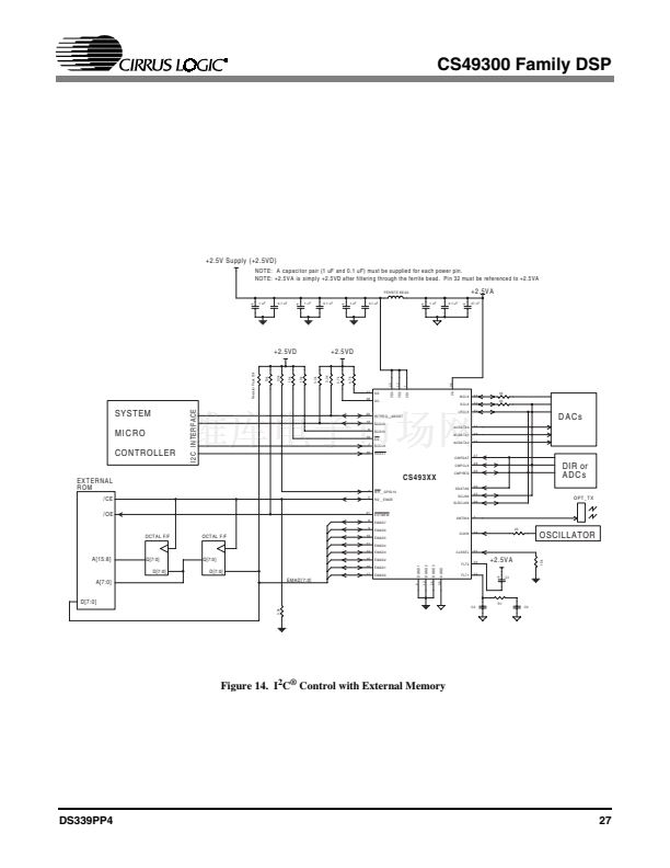
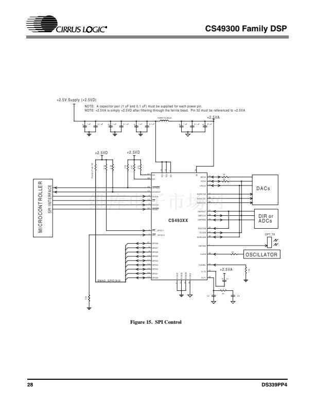
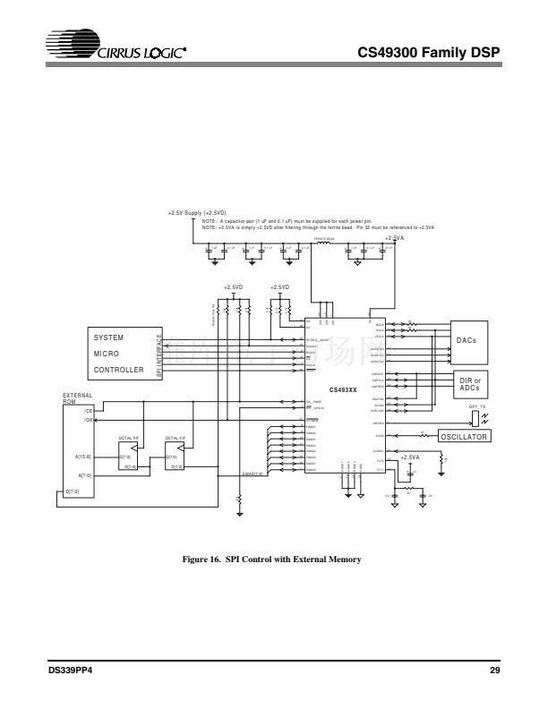
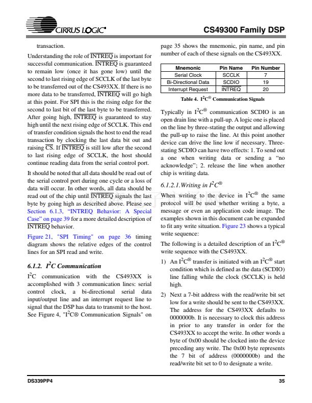
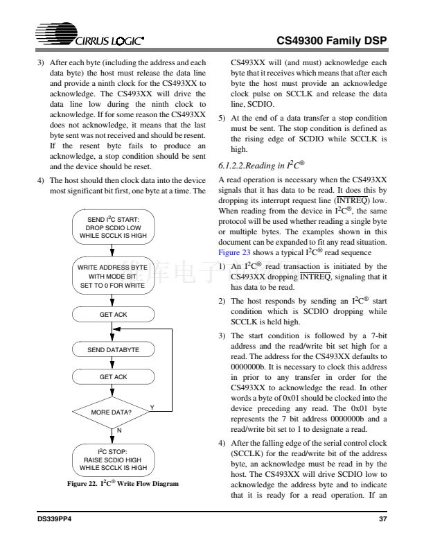
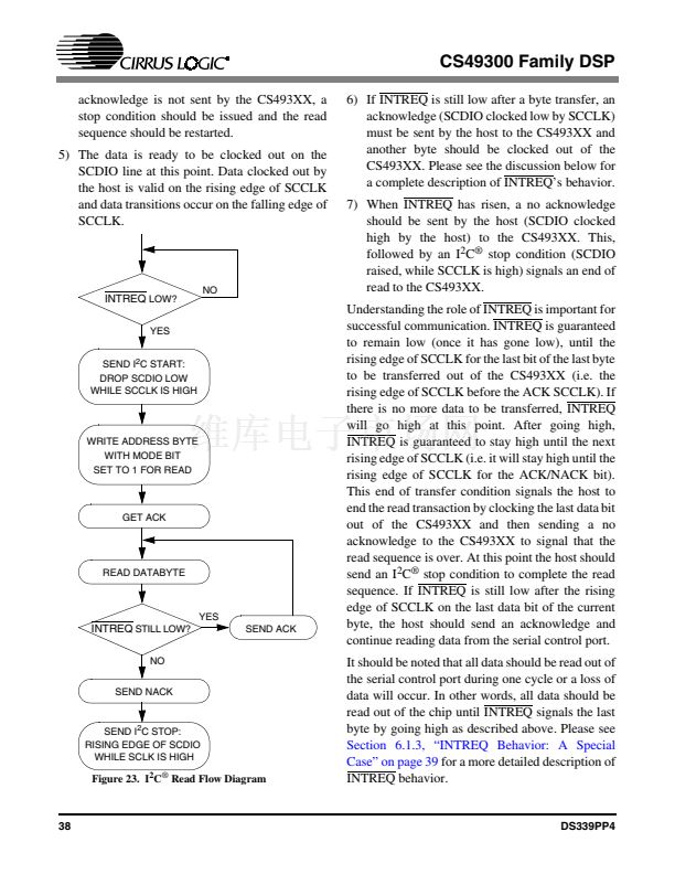
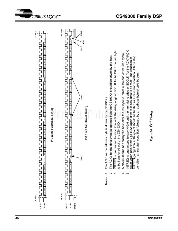
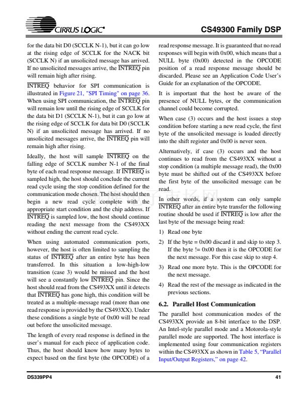
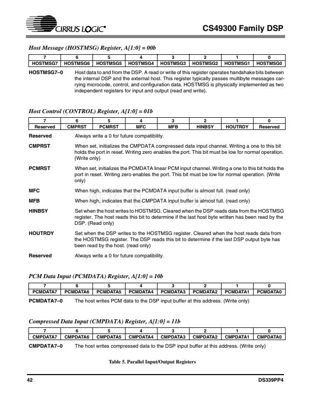
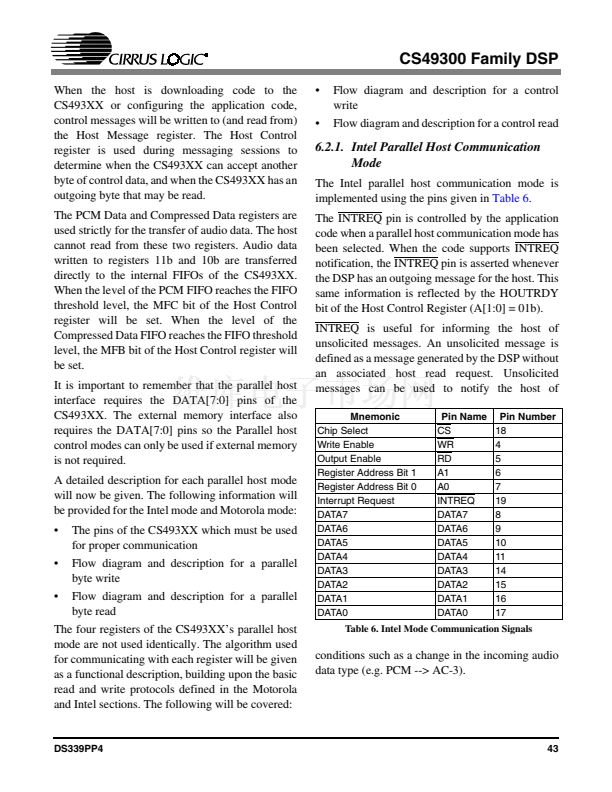
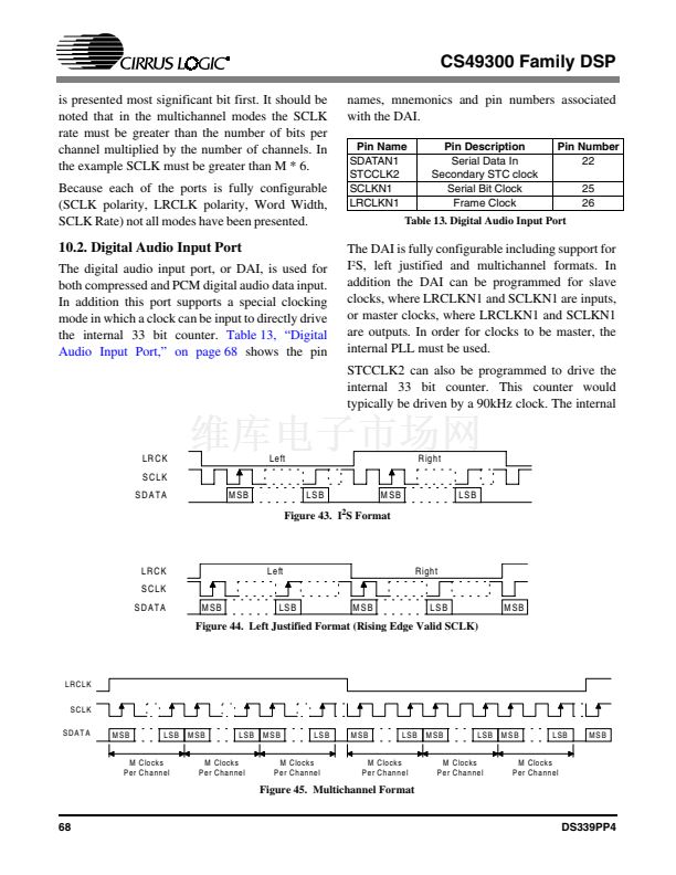
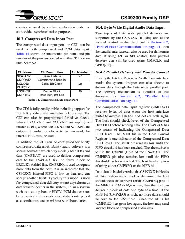
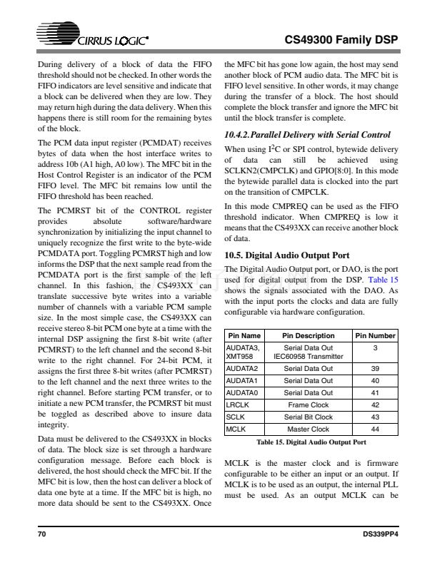
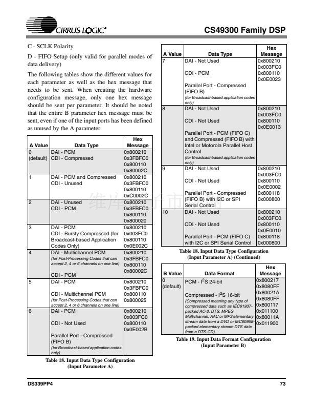
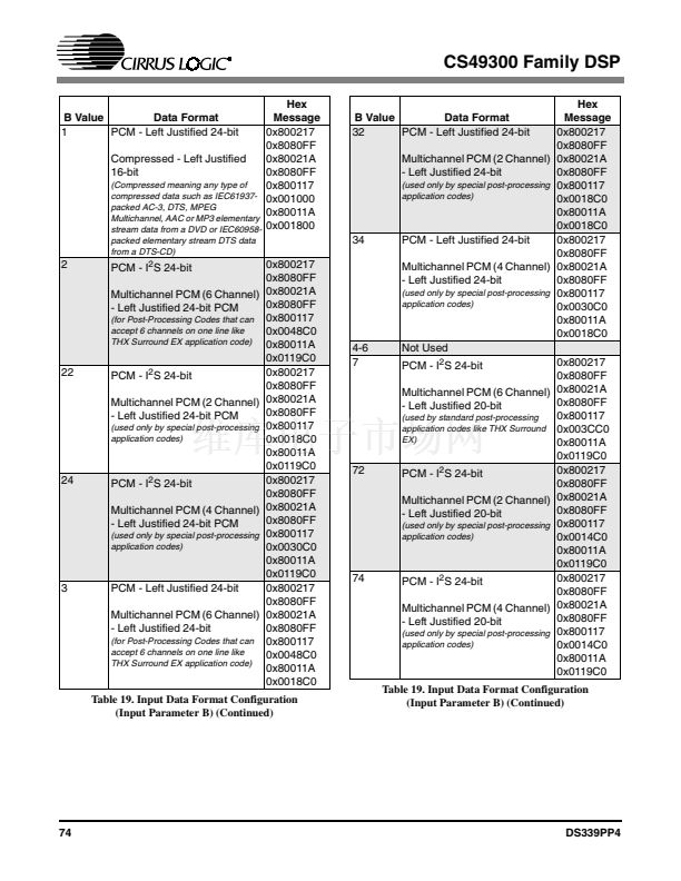
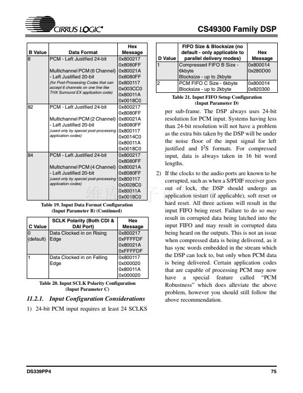
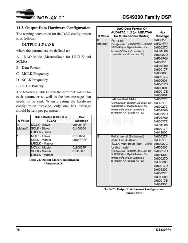
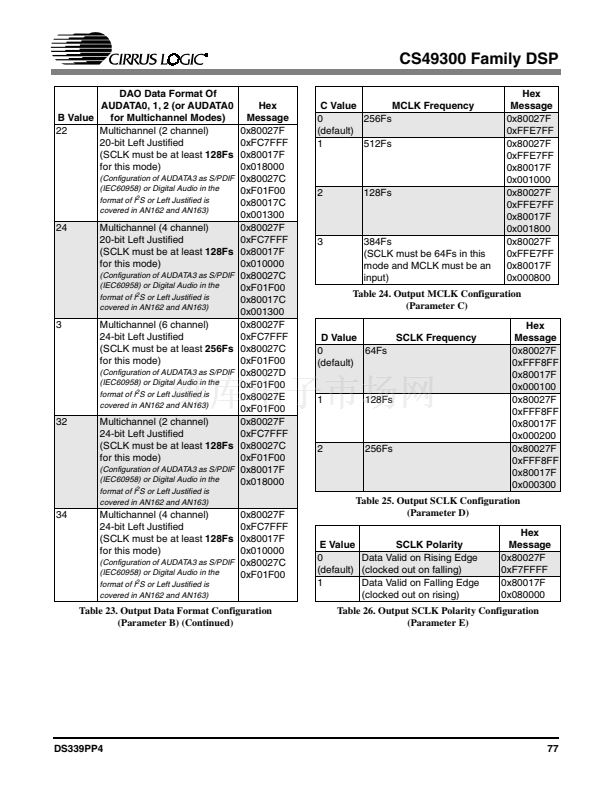
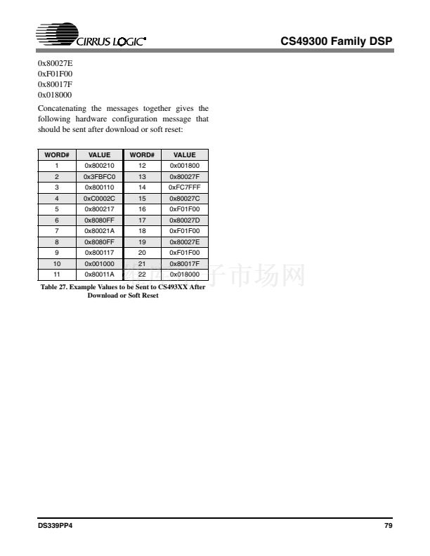
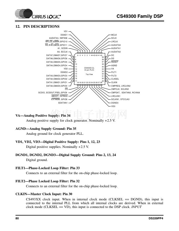
CS49300 Family DSP
name corresponding to their particular use.
Sometimes GPIO[11:0], or some subset thereof, is
used when referring to the pins in a general sense.
filter circuit will be directly coupled into the PLL,
which could affect performance.
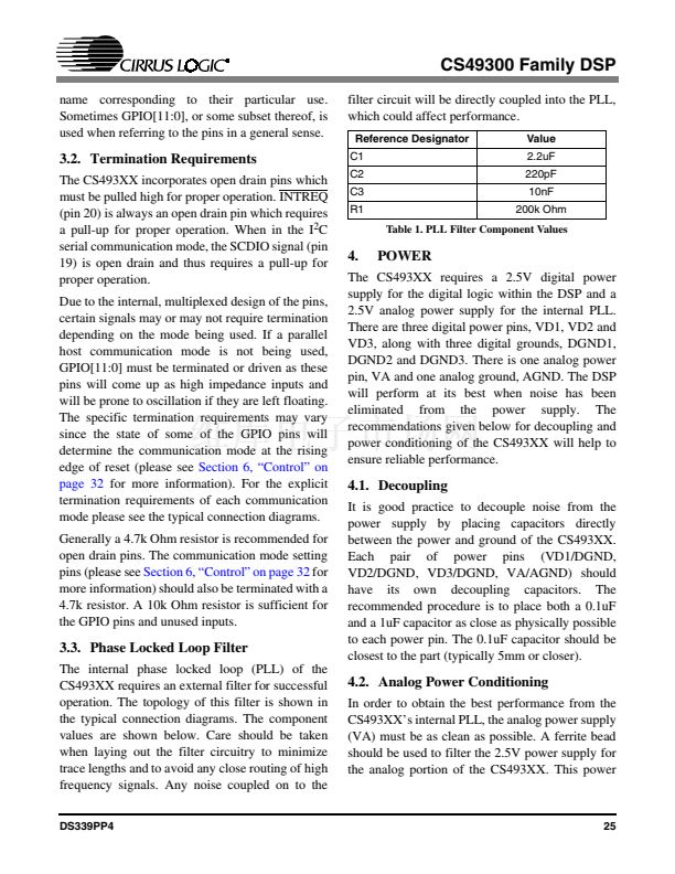
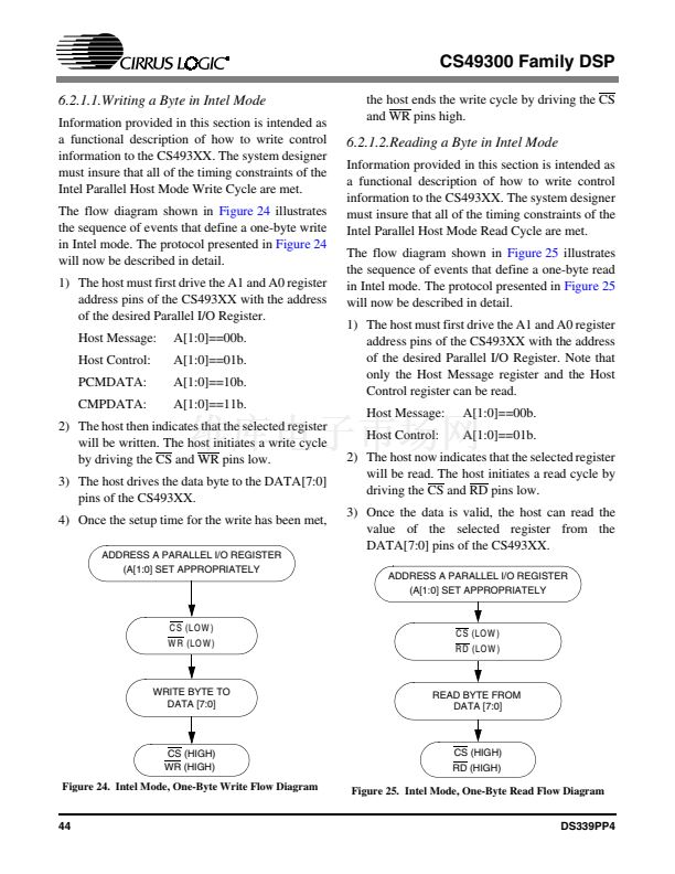
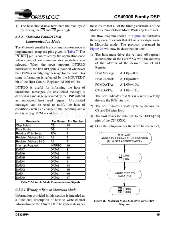
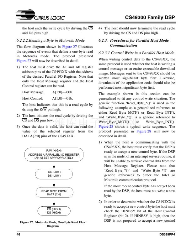
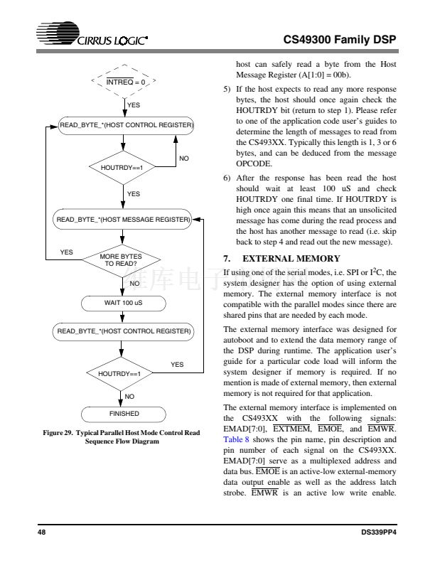
Reference Designator
C1
C2
C3
R1
Value
2.2uF
220pF
10nF
200k Ohm
Table 1. PLL Filter Component Values
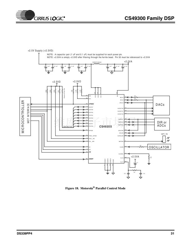
3.2. Termination Requirements
The CS493XX incorporates open drain pins which
must be pulled high for proper operation. INTREQ
(pin 20) is always an open drain pin which requires
a pull-up for proper operation. When in the I
2
C
serial communication mode, the SCDIO signal (pin
19) is open drain and thus requires a pull-up for
proper operation.
Due to the internal, multiplexed design of the pins,
certain signals may or may not require termination
depending on the mode being used. If a parallel
host communication mode is not being used,
GPIO[11:0] must be terminated or driven as these
pins will come up as high impedance inputs and
will be prone to oscillation if they are left floating.
The specific termination requirements may vary
since the state of some of the GPIO pins will
determine the communication mode at the rising
edge of reset (please see
Section 6, 鈥淐ontrol鈥?on
page 32
for more information). For the explicit
termination requirements of each communication
mode please see the typical connection diagrams.
Generally a 4.7k Ohm resistor is recommended for
open drain pins. The communication mode setting
pins (please see
Section 6, 鈥淐ontrol鈥?on page 32
for
more information) should also be terminated with a
4.7k resistor. A 10k Ohm resistor is sufficient for
the GPIO pins and unused inputs.
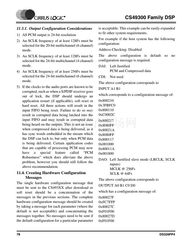
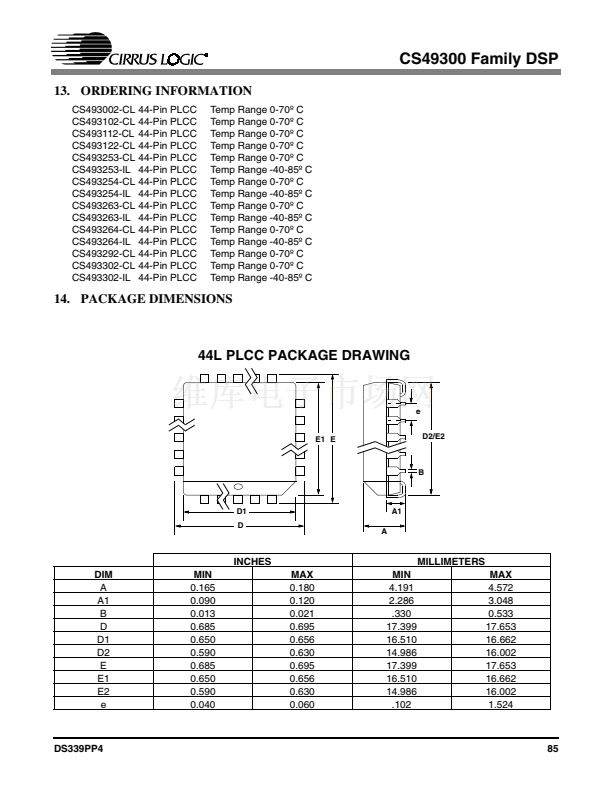
4.
POWER
The CS493XX requires a 2.5V digital power
supply for the digital logic within the DSP and a
2.5V analog power supply for the internal PLL.
There are three digital power pins, VD1, VD2 and
VD3, along with three digital grounds, DGND1,
DGND2 and DGND3. There is one analog power
pin, VA and one analog ground, AGND. The DSP
will perform at its best when noise has been
eliminated from the power supply. The
recommendations given below for decoupling and
power conditioning of the CS493XX will help to
ensure reliable performance.
4.1. Decoupling
It is good practice to decouple noise from the
power supply by placing capacitors directly
between the power and ground of the CS493XX.
Each pair of power pins (VD1/DGND,
VD2/DGND, VD3/DGND, VA/AGND) should
have its own decoupling capacitors. The
recommended procedure is to place both a 0.1uF
and a 1uF capacitor as close as physically possible
to each power pin. The 0.1uF capacitor should be
closest to the part (typically 5mm or closer).
3.3. Phase Locked Loop Filter
The internal phase locked loop (PLL) of the
CS493XX requires an external filter for successful
operation. The topology of this filter is shown in
the typical connection diagrams. The component
values are shown below. Care should be taken
when laying out the filter circuitry to minimize
trace lengths and to avoid any close routing of high
frequency signals. Any noise coupled on to the
DS339PP4
4.2. Analog Power Conditioning
In order to obtain the best performance from the
CS493XX鈥檚 internal PLL, the analog power supply
(VA) must be as clean as possible. A ferrite bead
should be used to filter the 2.5V power supply for
the analog portion of the CS493XX. This power
25


 1
1
 2
2
 3
3
 4
4
 5
5
 6
6
 7
7
 8
8
 9
9
 10
10
 11
11
 12
12
 13
13
 14
14
 15
15
 16
16
 17
17
 18
18
 19
19
 20
20
 21
21
 22
22
 23
23
 24
24
 25
25
 26
26
 27
27
 28
28
 29
29
 30
30
 31
31
 32
32
 33
33
 34
34
 35
35
 36
36
 37
37
 38
38
 39
39
 40
40
 41
41
 42
42
 43
43
 44
44
 45
45
 46
46
 47
47
 48
48
 49
49
 50
50
 51
51
 52
52
 53
53
 54
54
 55
55
 56
56
 57
57
 58
58
 59
59
 60
60
 61
61
 62
62
 63
63
 64
64
 65
65
 66
66
 67
67
 68
68
 69
69
 70
70
 71
71
 72
72
 73
73
 74
74
 75
75
 76
76
 77
77
 78
78
 79
79
 80
80
 81
81
 82
82
 83
83
 84
84
 85
85
 86
86
