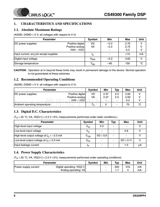
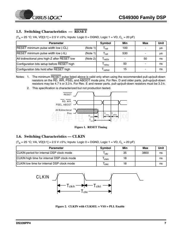
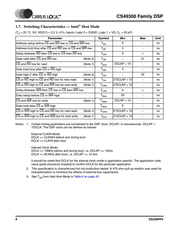
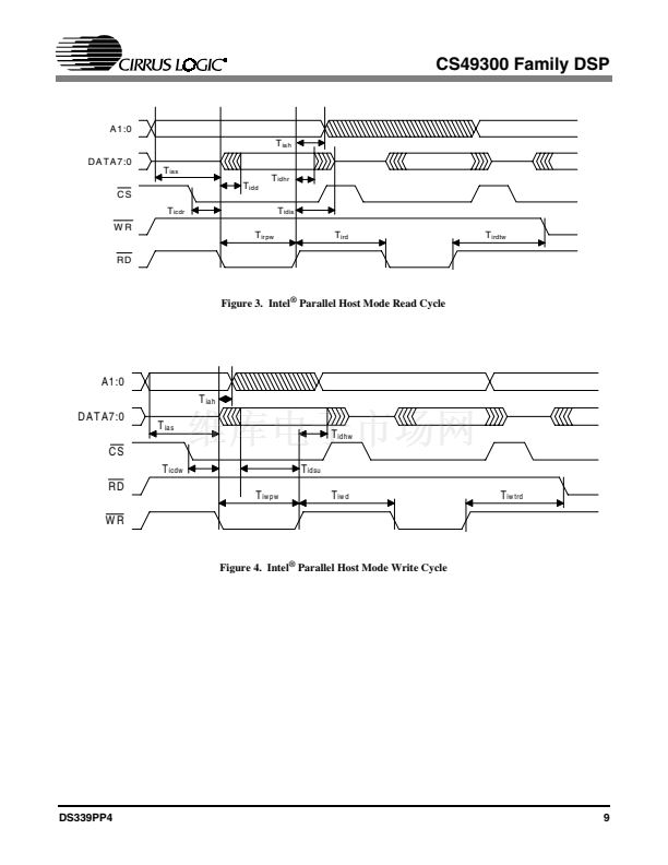
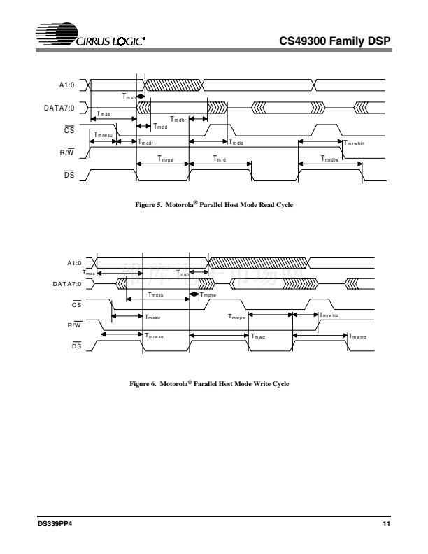
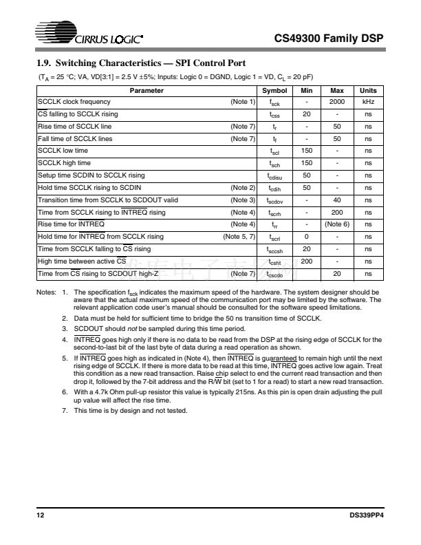
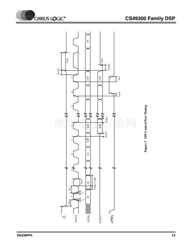
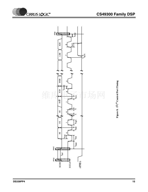
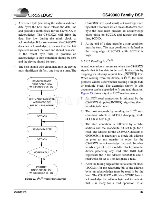
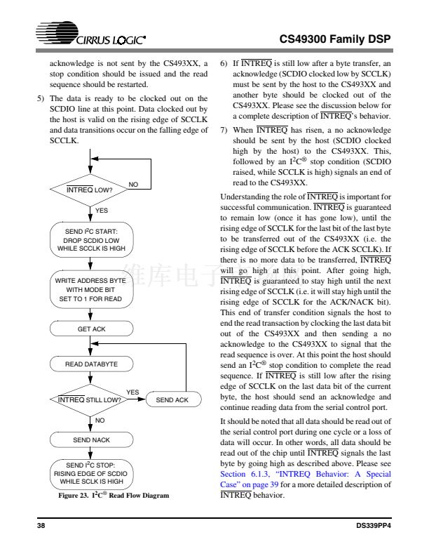
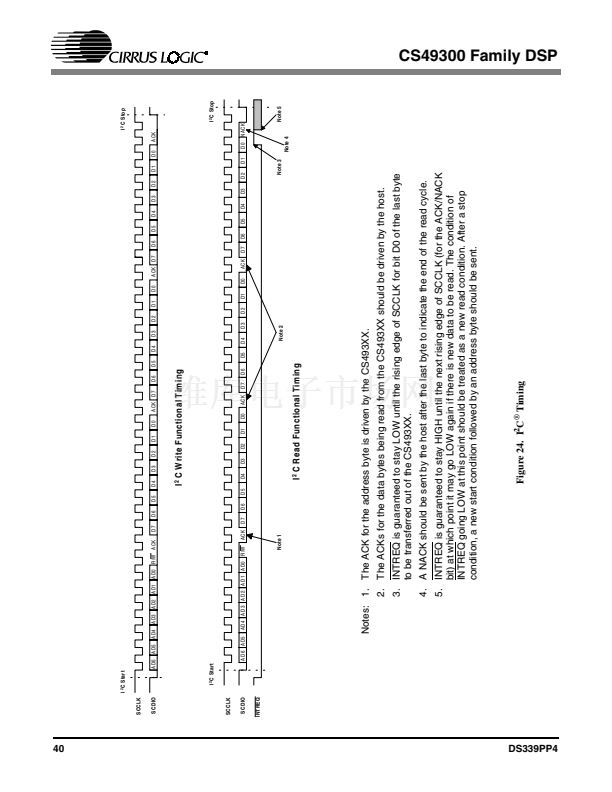
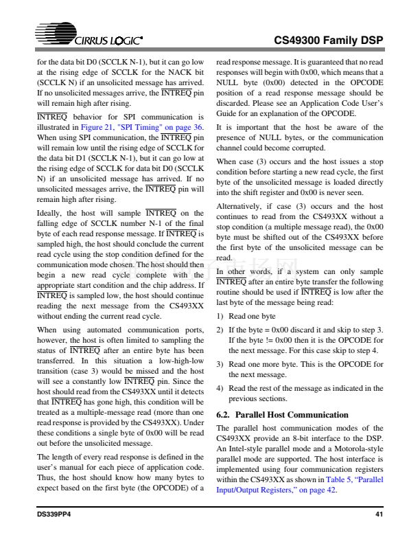
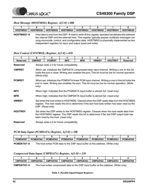
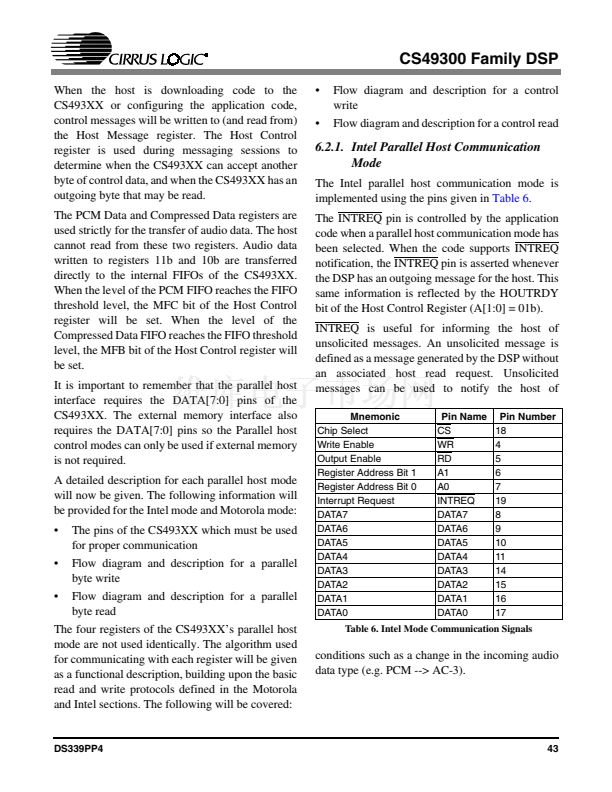
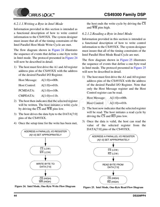
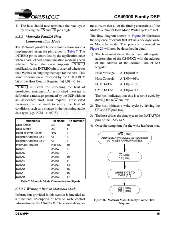
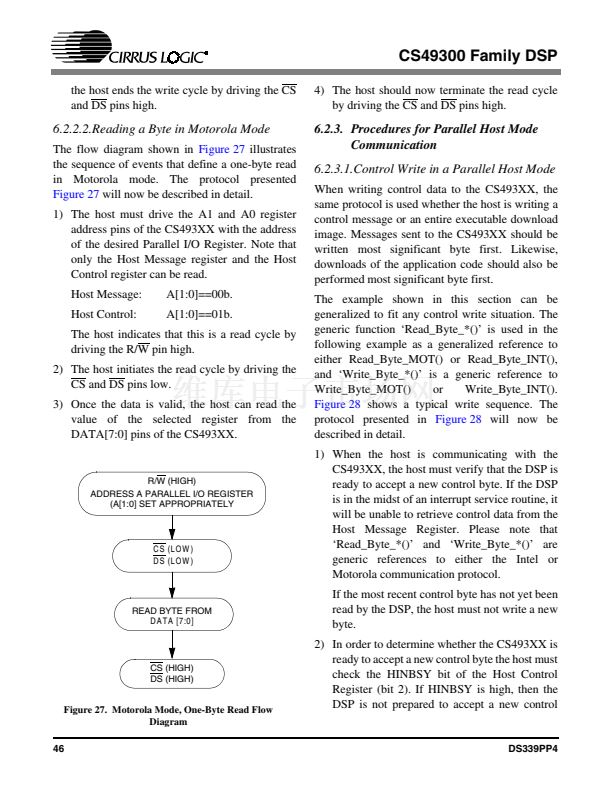
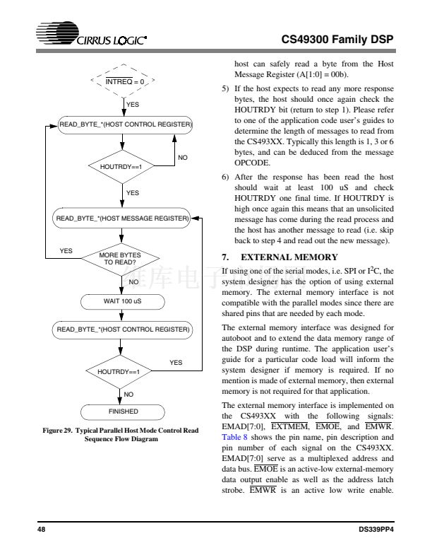
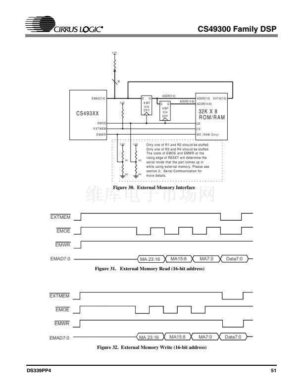
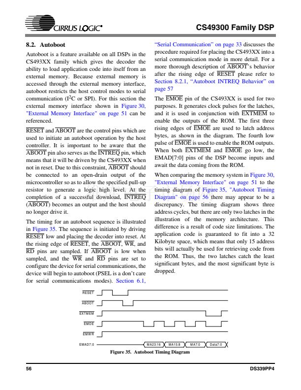
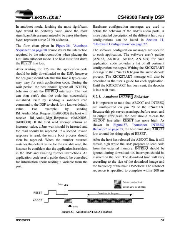
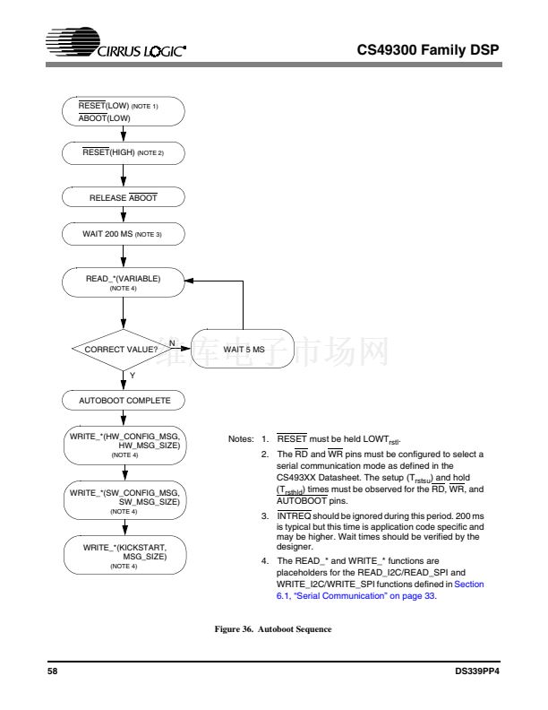
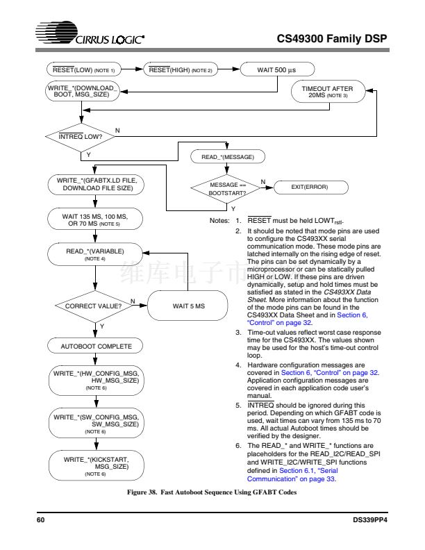
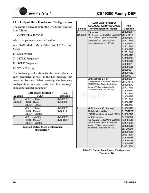
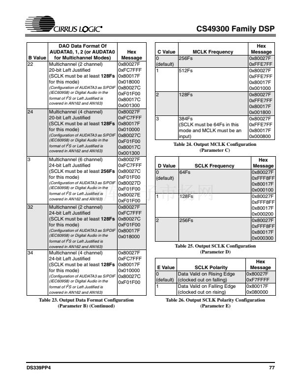
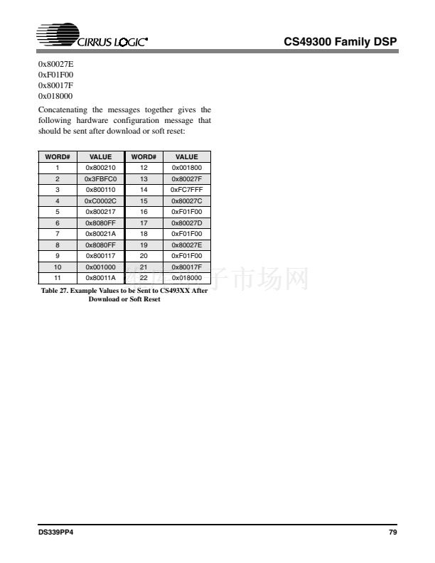
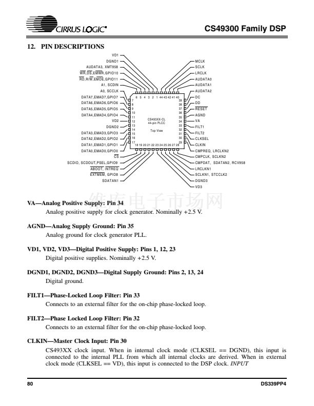
CS49300 Family DSP
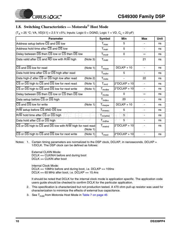
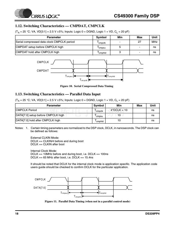
1.12. Switching Characteristics 鈥?CMPDAT, CMPCLK
(T
A
= 25
擄C;
VA, VD[3:1] = 2.5 V
鹵5%;
Inputs: Logic 0 = DGND, Logic 1 = VD, C
L
= 20 pF)
Parameter
Serial compressed data clock CMPCLK period
CMPDAT setup before CMPCLK high
CMPDAT hold after CMPCLK high
Symbol
T
cmpclk
T
cmpsu
T
cmphld
Min
-
5
3
Max
27
-
-
Unit
MHz
ns
ns
CM P CL K
CM P DA T
T
cm ps u
T
cm p clk
Figure 10. Serial Compressed Data Timing
T
cm p hld
1.13. Switching Characteristics 鈥?Parallel Data Input
(T
A
= 25
擄C;
VA, VD[3:1] = 2.5 V
鹵5%;
Inputs: Logic 0 = DGND, Logic 1 = VD, C
L
= 20 pF)
Parameter
CMPCLK Period
DATA[7:0] setup before CMPCLK high
DATA[7:0] hold after CMPCLK high
Symbol
T
cmpclk
T
cmpsu
T
cmphld
Min
4*DCLK + 10
10
10
Max
Unit
ns
ns
ns
Notes: 1. Certain timing parameters are normalized to the DSP clock, DCLK, in nanoseconds. The DSP clock can
be defined as follows:
External CLKIN Mode:
DCLK == CLKIN/4 before and during boot
DCLK == CLKIN after boot
Internal Clock Mode:
DCLK == 10MHz before and during boot, i.e. DCLK == 100ns
DCLK == 65 MHz after boot, i.e. DCLK == 15.4ns
It should be noted that DCLK for the internal clock mode is application specific. The application code
users guide should be checked to confirm DCLK for the particular application.
C M P C LK
D A T A [7:0]
T
cm psu
T
cm pclk
T
cm phld
Figure 11. Parallel Data Timing (when not in a parallel control mode)
18
DS339PP4


 1
1
 2
2
 3
3
 4
4
 5
5
 6
6
 7
7
 8
8
 9
9
 10
10
 11
11
 12
12
 13
13
 14
14
 15
15
 16
16
 17
17
 18
18
 19
19
 20
20
 21
21
 22
22
 23
23
 24
24
 25
25
 26
26
 27
27
 28
28
 29
29
 30
30
 31
31
 32
32
 33
33
 34
34
 35
35
 36
36
 37
37
 38
38
 39
39
 40
40
 41
41
 42
42
 43
43
 44
44
 45
45
 46
46
 47
47
 48
48
 49
49
 50
50
 51
51
 52
52
 53
53
 54
54
 55
55
 56
56
 57
57
 58
58
 59
59
 60
60
 61
61
 62
62
 63
63
 64
64
 65
65
 66
66
 67
67
 68
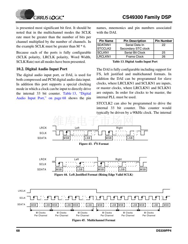
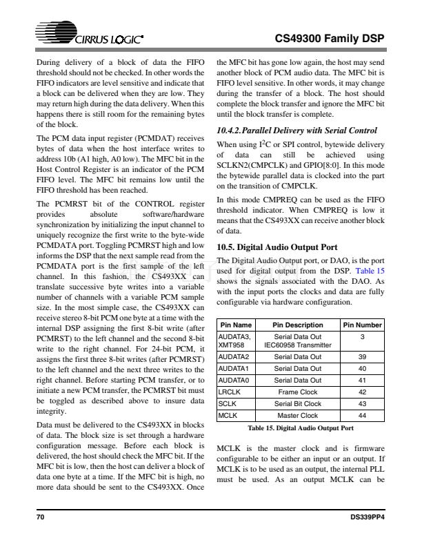
68
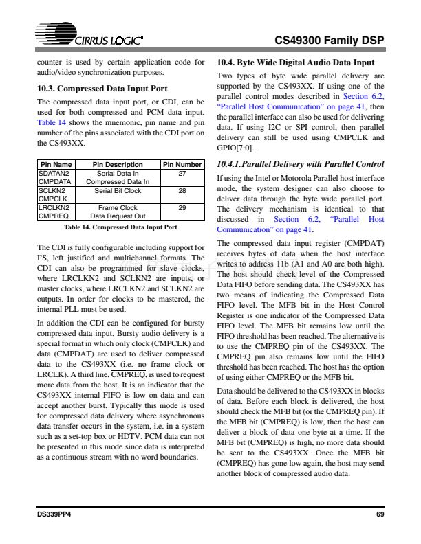 69
69
 70
70
 71
71
 72
72
 73
73
 74
74
 75
75
 76
76
 77
77
 78
78
 79
79
 80
80
 81
81
 82
82
 83
83
 84
84
 85
85
 86
86
