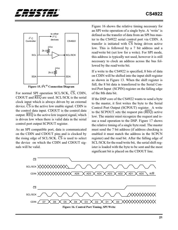
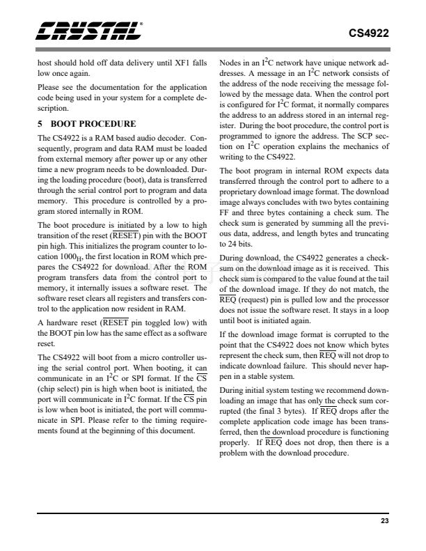
CS4922
If the CS4922 fails to ACK it is possible that the
byte was rejected and it should be transmitted
again. If the second attempt fails the CS4922
should be issued a hardware reset to reinitialize the
communication path.
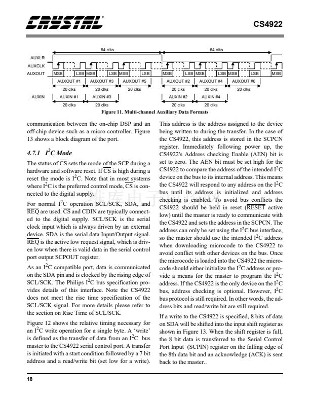
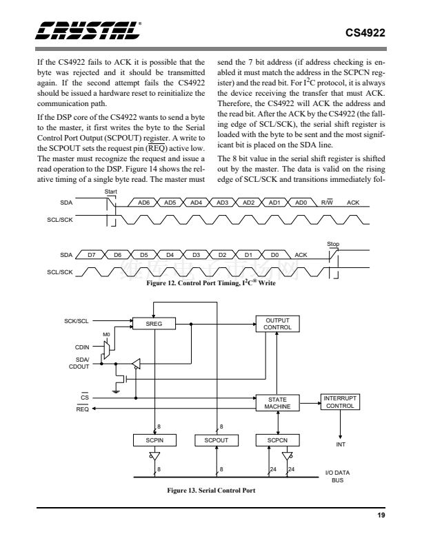
If the DSP core of the CS4922 wants to send a byte
to the master, it first writes the byte to the Serial
Control Port Output (SCPOUT) register. A write to
the SCPOUT sets the request pin (REQ) active low.
The master must recognize the request and issue a
read operation to the DSP. Figure 14 shows the rel-
ative timing of a single byte read. The master must
Start
SDA
SCL/SCK
AD6
AD5
AD4
AD3
AD2
send the 7 bit address (if address checking is en-
abled it must match the address in the SCPCN reg-
ister) and the read bit. For I
2
C protocol, it is always
the device receiving the transfer that must ACK.
Therefore, the CS4922 will ACK the address and
the read bit. After the ACK by the CS4922 (the fall-
ing edge of SCL/SCK), the serial shift register is
loaded with the byte to be sent and the most signif-
icant bit is placed on the SDA line.
The 8 bit value in the serial shift register is shifted
out by the master. The data is valid on the rising
edge of SCL/SCK and transitions immediately fol-
AD1
AD0
R/W
ACK
Stop
SDA
D7
D6
D5
D4
D3
D2
D1
D0
ACK
SCL/SCK
Figure 12. Control Port Timing, I
2
C
廬
Write
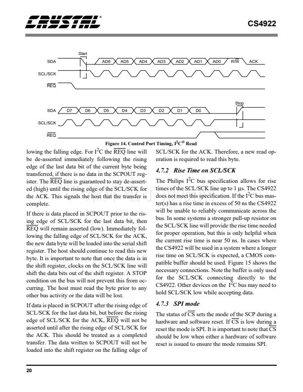
SCK/SCL
M0
SREG
OUTPUT
CONTROL
CDIN
SDA/
CDOUT
CS
REQ
8
8
STATE
MACHINE
INTERRUPT
CONTROL
SCPIN
SCPOUT
SCPCN
INT
8
8
24
24
I/O DATA
BUS
Figure 13. Serial Control Port
19


 1
1
 2
2
 3
3
 4
4
 5
5
 6
6
 7
7
 8
8
 9
9
 10
10
 11
11
 12
12
 13
13
 14
14
 15
15
 16
16
 17
17
 18
18
 19
19
 20
20
 21
21
 22
22
 23
23
 24
24
 25
25
 26
26
 27
27
 28
28
 29
29
 30
30
 31
31
 32
32
 33
33
 34
34
