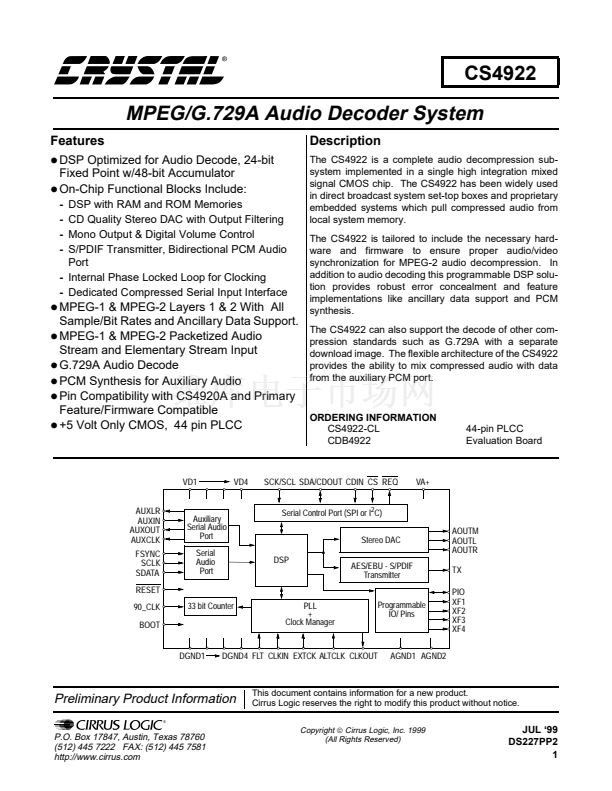
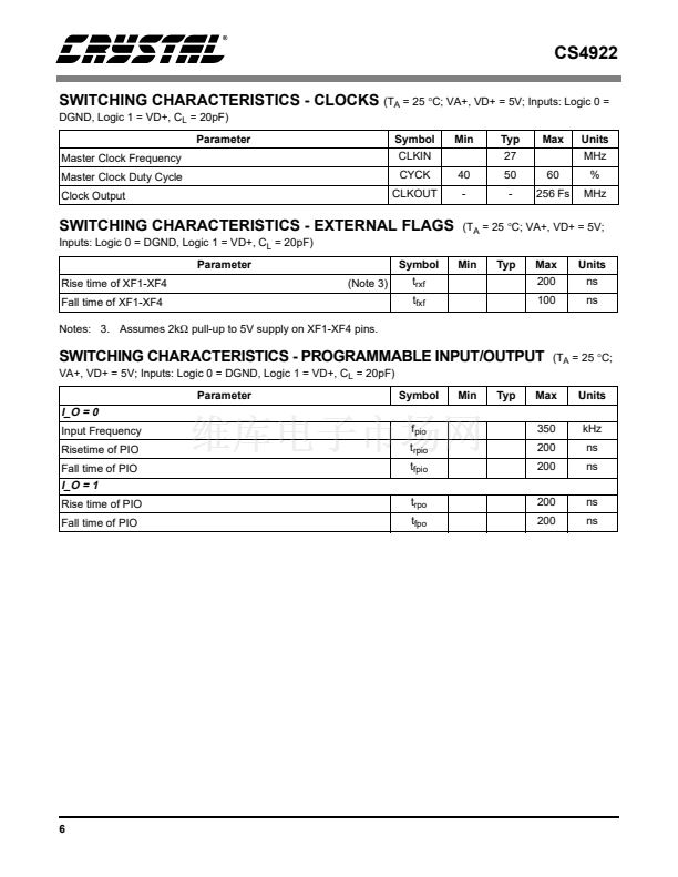
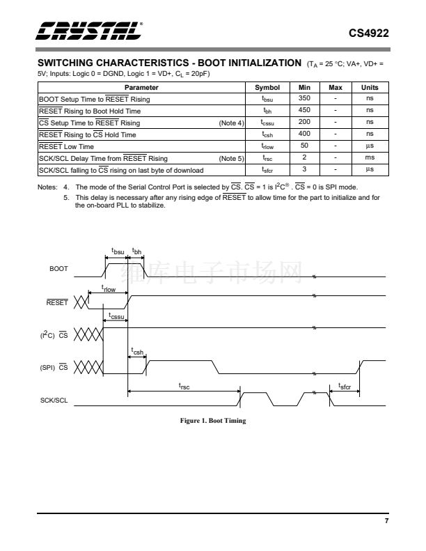
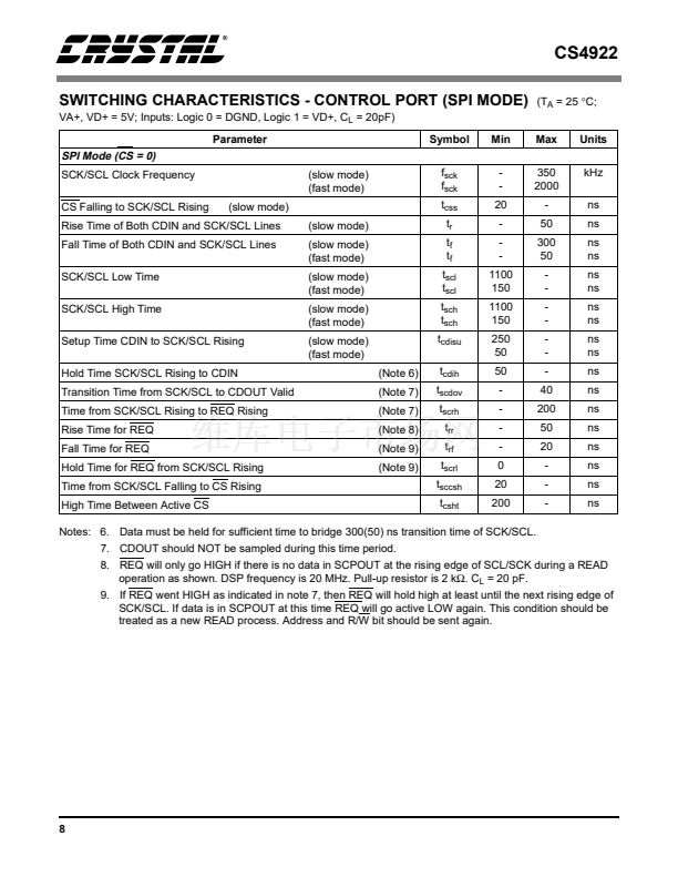
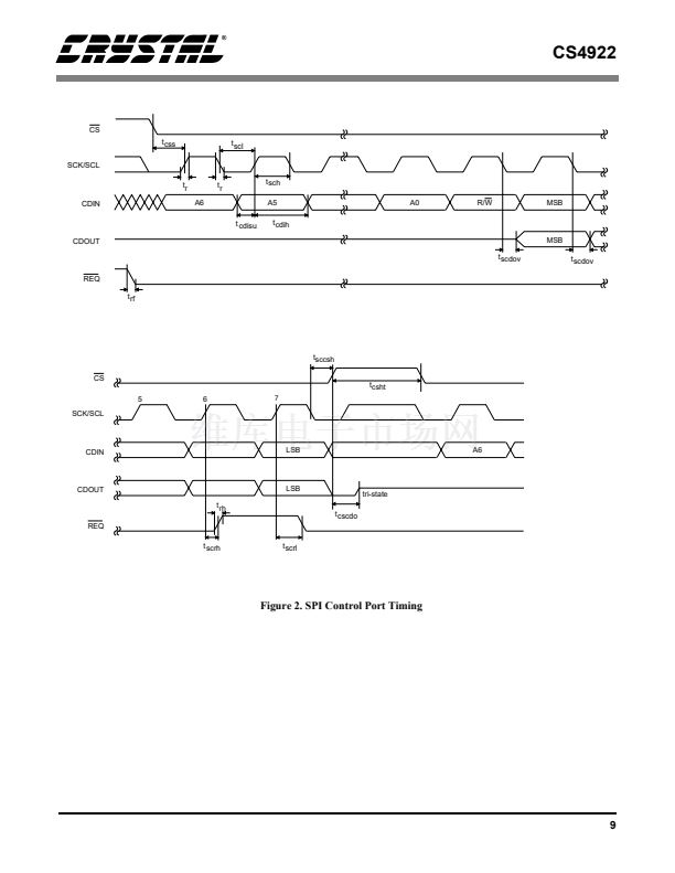
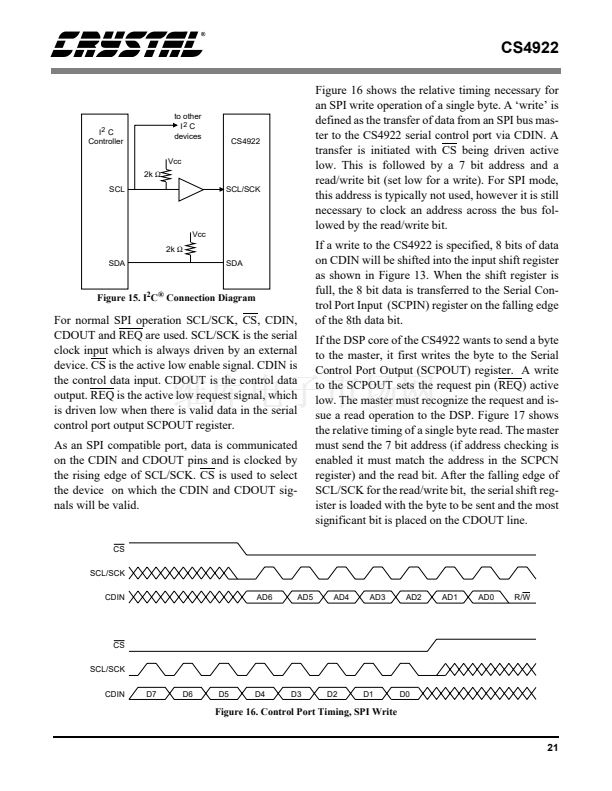
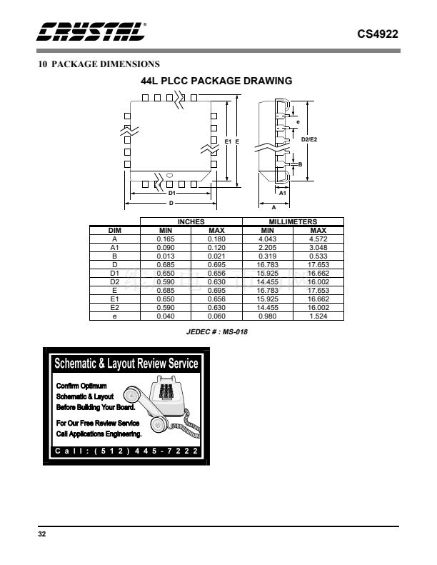
CS4922
64 clks
AUXLR
AUXCLK
AUXOUT
MSB
LSB MSB
LSB MSB
LSB
MSB
LSB MSB
LSB MSB
LSB
MSB
64 clks
AUXOUT #1
20 clks
AUXIN
AUXIN #1
AUXOUT #3
20 clks
AUXIN #3
AUXOUT #5
20 clks
AUXOUT #2
20 clks
AUXIN #2
AUXOUT #4
20 clks
AUXIN #4
AUXOUT #6
20 clks
20 clks
20 clks
20 clks
20 clks
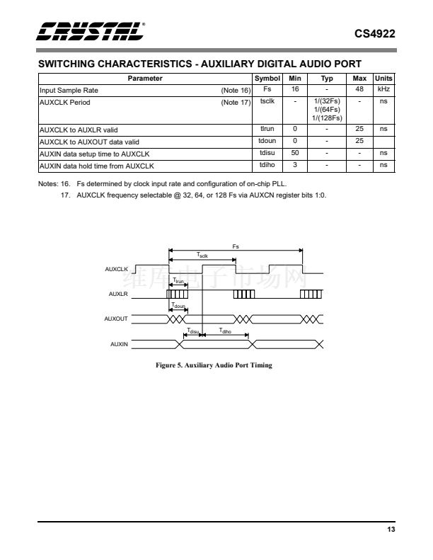
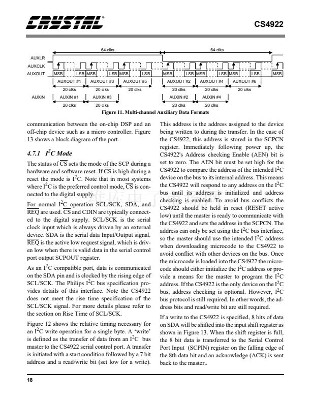
Figure 11. Multi-channel Auxiliary Data Formats
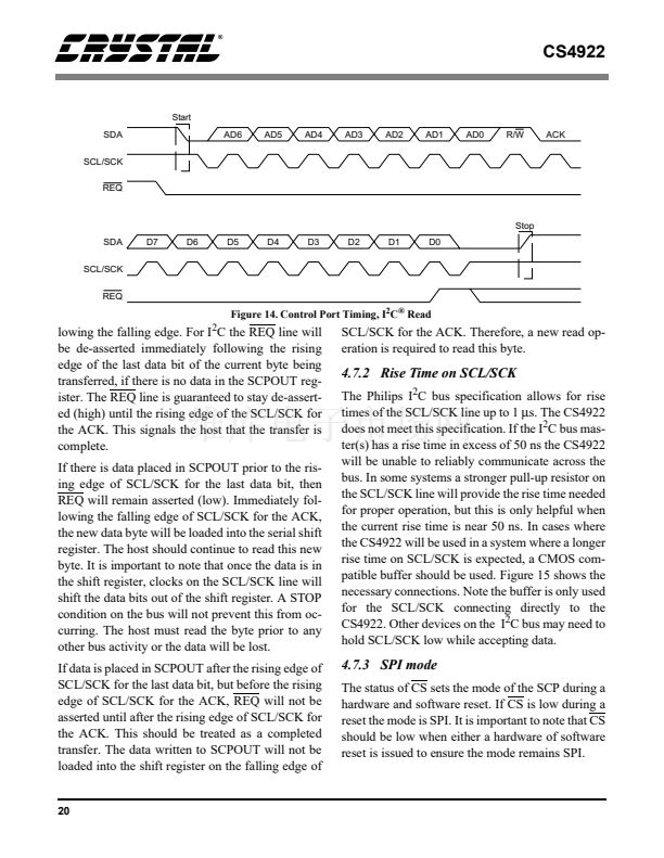
communication between the on-chip DSP and an
off-chip device such as a micro controller. Figure
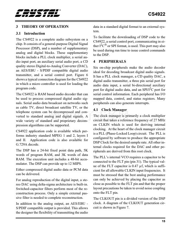
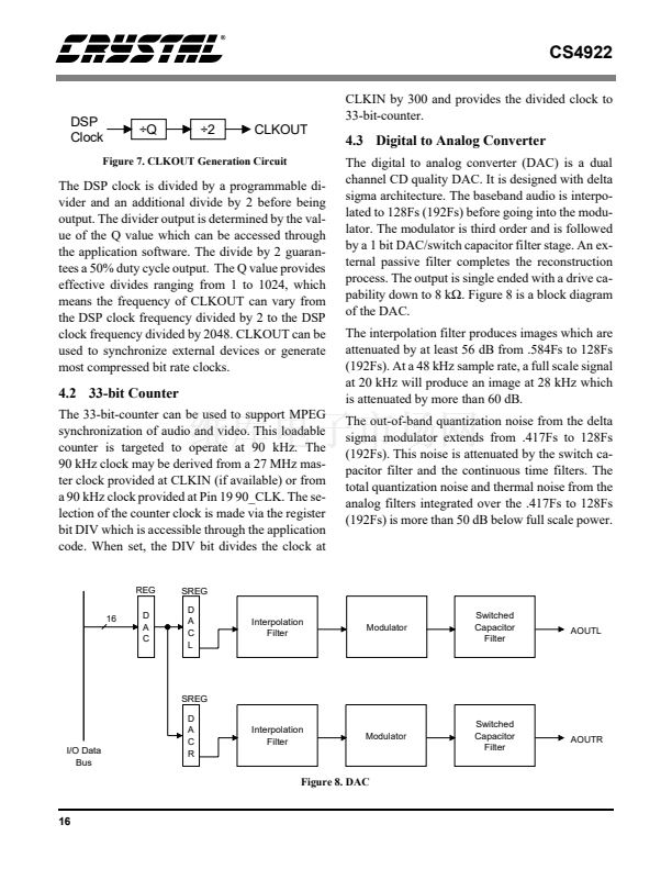
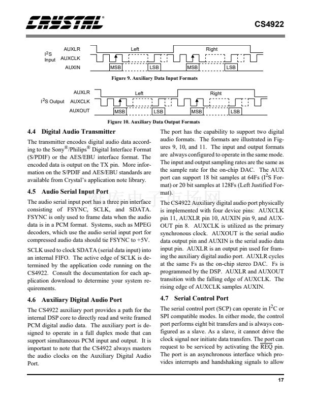
13 shows a block diagram of the port.
4.7.1 I
2
C Mode
The status of CS sets the mode of the SCP during a
hardware and software reset. If CS is high during a
reset the mode is I
2
C. Note that in most systems
where I
2
C is the preferred control mode, CS is con-
nected to the digital supply.
For normal I
2
C operation SCL/SCK, SDA, and
REQ are used. CS and CDIN are typically connect-
ed to the digital supply. SCL/SCK is the serial
clock input which is always driven by an external
device. SDA is the serial data Input/Output signal.
REQ is the active low request signal, which is driv-
en low when there is valid data in the serial control
port output SCPOUT register.
As an I
2
C compatible port, data is communicated
on the SDA pin and is clocked by the rising edge of
SCL/SCK. The Philips I
2
C bus specification pro-
vides details of this interface. Note the CS4922
does not meet the rise time specification of the
SCL/SCK signal. For more details please refer to
the section on Rise Time of SCL/SCK.
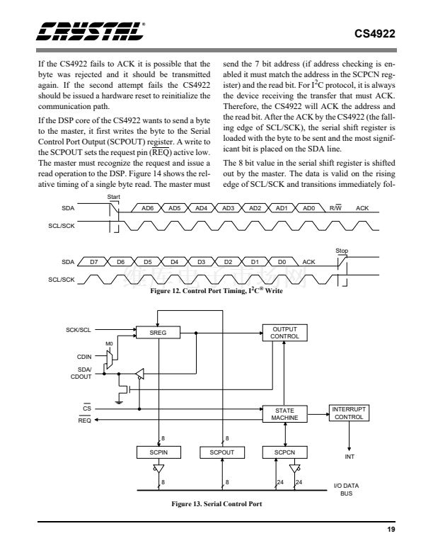
Figure 12 shows the relative timing necessary for
an I
2
C write operation for a single byte. A 鈥榳rite鈥?/div>
is defined as the transfer of data from an I
2
C bus
master to the CS4922 serial control port. A transfer
is initiated with a start condition followed by a 7 bit
address and a read/write bit (set low for a write).
18
This address is the address assigned to the device
being written to during the transfer. In the case of
the CS4922, this address is stored in the SCPCN
register. Immediately following power up, the
CS4922's Address checking Enable (AEN) bit is
set to zero. The AEN bit must be set high for the
CS4922 to compare the address of the intended I
2
C
device on the bus to its internal address. This means
the CS4922 will respond to any address on the I
2
C
bus until its address is initialized and address
checking is enabled. To avoid bus conflicts the
CS4922 should be held in reset (RESET active
low) until the master is ready to communicate with
the CS4922 and sets the address in the SCPCN. The
address can only be set using the I
2
C bus interface,
so the master should use the intended I
2
C address
when downloading microcode to the CS4922 to
avoid conflict with other devices on the bus. Once
the microcode is loaded into the CS4922 the micro-
code should either initialize the I
2
C address or pro-
vide a means for the master to program the I
2
C
address. If the CS4922 is the only device on the I
2
C
bus, address checking is optional. However, I
2
C
bus protocol is still required. In other words, the ad-
dress bits and read/write bit are still required.
If a write to the CS4922 is specified, 8 bits of data
on SDA will be shifted into the input shift register as
shown in Figure 13. When the shift register is full,
the 8 bit data is transferred to the Serial Control
Port Input (SCPIN) register on the falling edge of
the 8th data bit and an acknowledge (ACK) is sent
back to the master..


 1
1
 2
2
 3
3
 4
4
 5
5
 6
6
 7
7
 8
8
 9
9
 10
10
 11
11
 12
12
 13
13
 14
14
 15
15
 16
16
 17
17
 18
18
 19
19
 20
20
 21
21
 22
22
 23
23
 24
24
 25
25
 26
26
 27
27
 28
28
 29
29
 30
30
 31
31
 32
32
 33
33
 34
34
