鈩?/div>
and be properly
terminated at each end using surface mount components.
Careful layout is imperative to minimize crosstalk. Guards
(ground or supply traces) must be run between all signal traces
to limit direct capacitive coupling. Input and output signal lines
should fan out away from the mux as much as possible. If
multiple signal layers are available, a buried stripline structure
having ground plane above, below, and between signal traces
will have the best crosstalk performance.
Return currents flowing through termination resistors can also
increase crosstalk if these currents flow in sections of the finite-
impedance ground circuit that is shared between more than one
input or output. Minimizing the inductance and resistance of the
ground plane can reduce this effect, but further care should be
taken in positioning the terminations. Terminating cables directly
at the connectors will minimize the return current flowing on the
board, but the signal trace between the connector and the mux will
look like an open stub and will degrade the frequency response.
Moving the termination resistors close to the input pins will
improve the frequency response, but the terminations from
neighboring inputs should not have a common ground return.
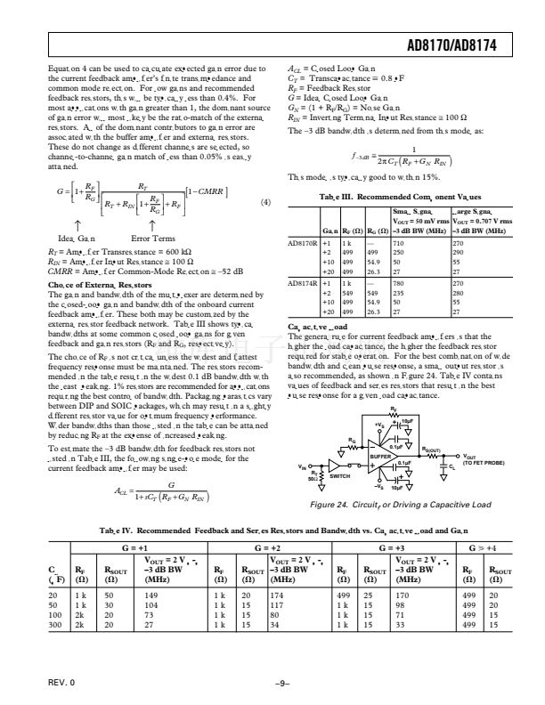
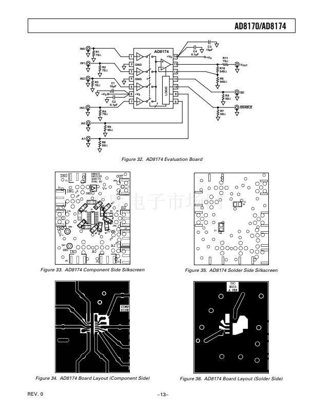
APPLICATIONS
8-to-1 Video Multiplexer
Realizing the high speed performance attainable with the
AD8170 and AD8174 requires careful attention to board layout
and component selection. Proper RF design techniques and low
parasitic component selection are mandatory.
Wire wrap boards, prototype boards, and sockets are not
recommended because of their high parasitic inductance and
capacitance. Instead, surface-mount components should be
soldered directly to a printed circuit board (PCB). The PCB
should have a ground plane covering all unused portions of the
component side of the board to provide a low impedance
ground path. The ground plane should be removed from the
area near input and output pins to reduce stray capacitance.
Chip capacitors should be used for supply bypassing. One end
of the capacitor should be connected to the ground plane and
the other within 1/4 inch of each power pin. An additional large
(4.7
碌F鈥?0 碌F)
tantalum capacitor should be connected in
parallel with each of the smaller capacitors for low impedance
supply bypassing over a broad range of frequencies.
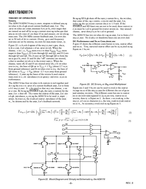
Two AD8174 4-to-1 multiplexers can be combined with a single
digital inverter to yield an 8-to-1 multiplexer as shown in Figure
26. The
ENABLE
control pin allows the two op amp outputs to
be connected together directly. Taking the
ENABLE
pin high
shuts off the supply current to the output op amp and places the
op amp鈥檚 output and inverting input (Pin 12, 鈥揤
IN
) in high
impedance states.
The two least significant bits (LSBs) of the address lines
connect directly to the A0 and A1 inputs of both AD8174
devices. The third address line connects directly to the
ENABLE
input on one device and is inverted before being
applied to the
ENABLE
input on the second device. As a
result, when one device is enabled, the second device presents a
high impedance. The op amp of the enabled device must
however drive both feedback networks ((549
鈩?/div>
+ 549
鈩?/2).
The gain of this multiplexer has been set to +2 in this example.
This gives an overall gain of +1 when back terminated lines are
used. In applications where switching and settling times are
critical, the digital control pins (A0, A1 and
ENABLE)
should
also be appropriately terminated (with either 50


 1
1
 2
2
 3
3
 4
4
 5
5
 6
6
 7
7
 8
8
 9
9
 10
10
 11
11
 12
12
 13
13
 14
14
 15
15
 16
16
