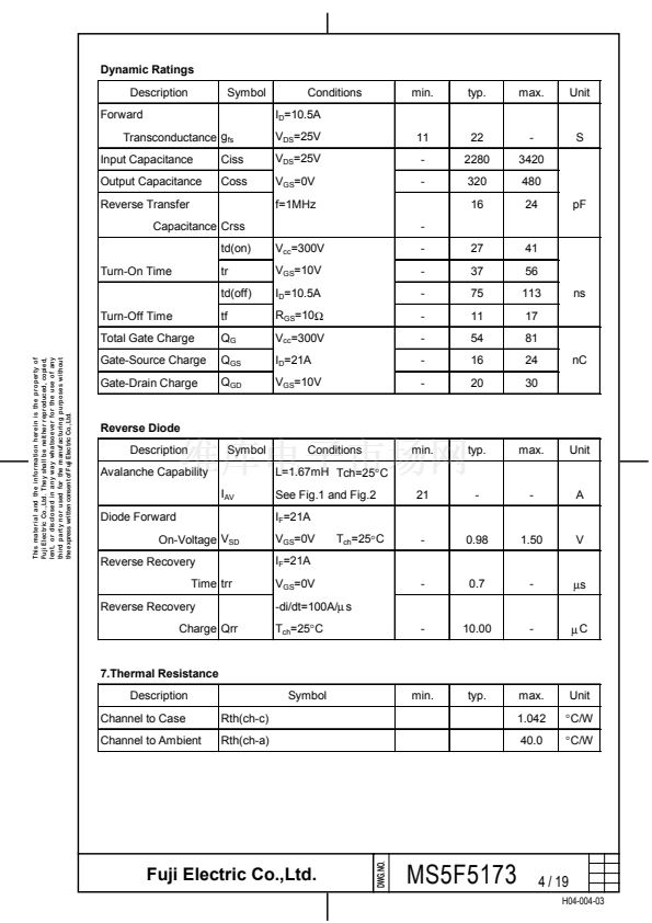
Dynamic Ratings
Description
Forward
Transconductance g
fs
Input Capacitance
Output Capacitance
Reverse Transfer
Capacitance Crss
td(on)
Turn-On Time
tr
td(off)
Turn-Off Time
Total Gate Charge
This material and the information herein is the property of
Fuji Electric Co.,Ltd. They shall be neither reproduced, copied,
lent, or disclosed in any way whatsoever for the use of any
third party nor used for the manufacturing purposes without
the express written consent of Fuji Electric Co.,Ltd.
Symbol
Conditions
I
D
=10.5A
V
DS
=25V
V
DS
=25V
V
GS
=0V
f=1MHz
min.
typ.
max.
Unit
11
-
-
22
2280
320
16
-
3420
480
24
S
Ciss
Coss
pF
-
V
cc
=300V
V
GS
=10V
I
D
=10.5A
R
GS
=10鈩?/div>
V
cc
=300V
I
D
=21A
V
GS
=10V
-
-
-
-
-
-
-
27
37
75
11
54
16
20
41
56
113
17
81
24
30
nC
ns
tf
Q
G
Q
GS
Q
GD
Gate-Source Charge
Gate-Drain Charge
Reverse Diode
Description
Avalanche Capability
I
AV
Diode Forward
On-Voltage V
SD
Reverse Recovery
Time trr
Reverse Recovery
Charge Qrr
Symbol
Conditions
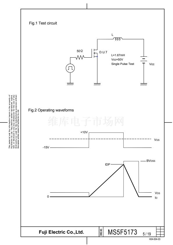
L=1.67mH Tch=25擄C
See Fig.1 and Fig.2
I
F
=21A
V
GS
=0V
I
F
=21A
V
GS
=0V
-di/dt=100A/碌 s
T
ch
=25擄C
-
10.00
-
碌
C
-
0.7
-
碌s
T
ch
=25擄C
-
0.98
1.50
V
21
-
-
A
min.
typ.
max.
Unit
7.Thermal Resistance
Description
Channel to Case
Channel to Ambient
Rth(ch-c)
Rth(ch-a)
Symbol
min.
typ.
max.
1.042
40.0
Unit
擄C/W
擄C/W
Fuji Electric Co.,Ltd.
MS5F5173
DWG.NO.
4 / 19
H04-004-03


 1
1
 2
2
 3
3
 4
4
 5
5
 6
6
 7
7
 8
8
 9
9
 10
10
 11
11
 12
12
 13
13
 14
14
 15
15
 16
16
 17
17
 18
18
 19
19
