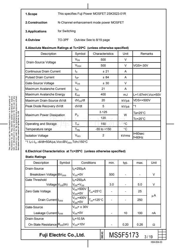
1.Scope
2.Construction
3.Applications
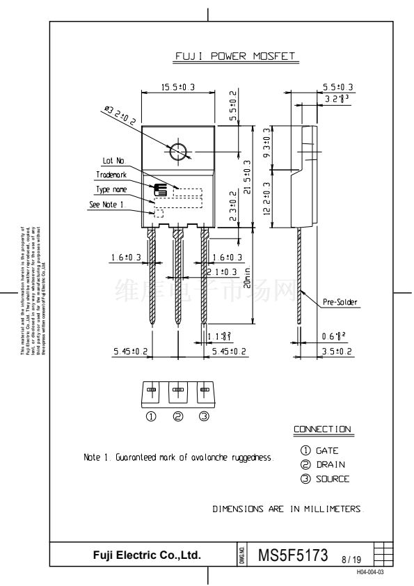
4.Outview
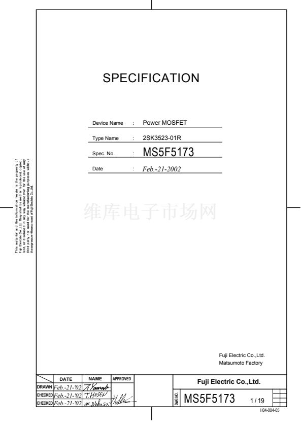
This specifies Fuji Power MOSFET 2SK3523-01R
N-Channel enhancement mode power MOSFET
for Switching
TO-3PF
Outview See to 8/19 page
5.Absolute Maximum Ratings at Tc=25擄 C (unless otherwise specified)
擄
Description
Drain-Source Voltage
Continuous Drain Current
Pulsed Drain Current
Gate-Source Voltage
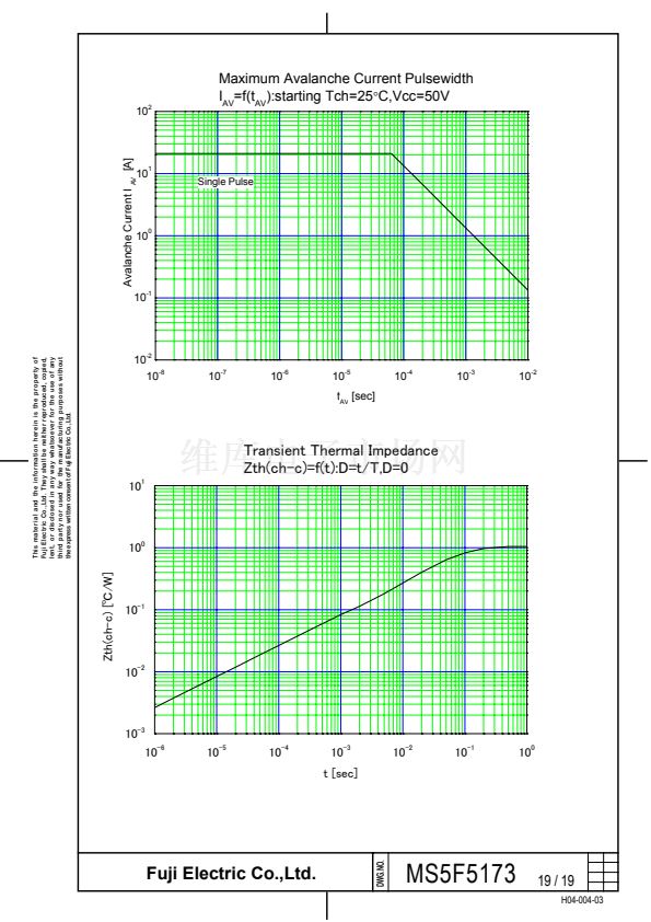
Maximum Avalanche Current
This material and the information herein is the property of
Fuji Electric Co.,Ltd. They shall be neither reproduced, copied,
lent, or disclosed in any way whatsoever for the use of any
third party nor used for the manufacturing purposes without
the express written consent of Fuji Electric Co.,Ltd.
Symbol
V
DS
V
DSX
I
D
I
DP
V
GS
I
AS
E
AS
dV
DS
/dt
dV/dt
P
D
T
ch
T
stg
V
ISO
Characteristics
500
500
鹵 21
鹵 84
鹵 30
21
400
20
5
3.125
120
150
-55 to +150
2
Unit
V
V
A
A
V
A
mJ
kV/碌s
kV/碌s
W
擄C
擄C
kVrms
Remarks
VGS=-30V
Maximum Avalanche Energy
Maximum Drain-Source dV/dt
Peak Diode Recovery dV/dt
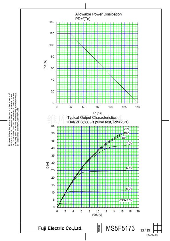
Maximum Power Dissipation
Operating and Storage
Temperature range
Isolation Voltage
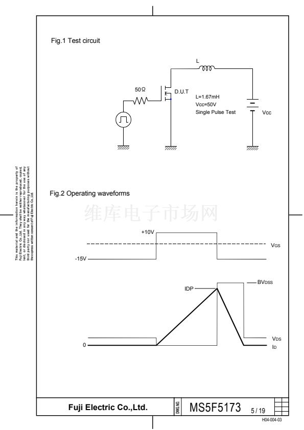
L=1.67mH,Vcc=50V
VDS<=500V
*1
Ta=25擄C
Tc=25擄C
t=60sec
f=60Hz
*1 I
F
鈮?I
D
,-di/dt=50A/碌s,Vcc鈮V
DSS
,Tch鈮?50擄C
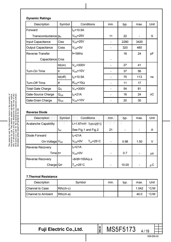
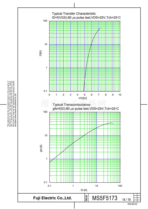
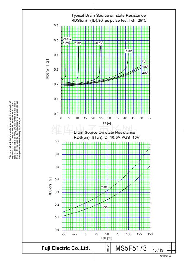
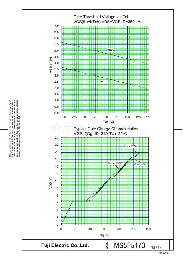
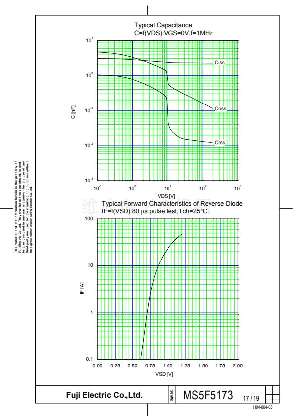
6.Electrical Characteristics at Tc=25擄 C (unless otherwise specified)
擄
Static Ratings
Description
Drain-Source
Breakdown Voltage BV
DSS
Gate Threshold
Voltage V
GS
(th)
Zero Gate Voltage
Drain Current I
DSS
Gate-Source
Leakage Current I
GSS
Drain-Source
On-State Resistance R
DS
(on)
Symbol
Conditions
I
D
=250碌A
V
GS
=0V
I
D
=250碌A
V
DS
=V
GS
V
DS
=500V
T
ch
=25擄C
V
GS
=0V
V
DS
=400V
T
ch
=125擄C
V
GS
=0V
V
GS
= 鹵 30V
V
DS
=0V
I
D
=10.5A
V
GS
=10V
DWG.NO.
min.
typ.
max.
Unit
500
3.0
-
-
-
-
-
-
-
5.0
25
V
V
碌
A
250
-
10
100
nA
-
0.20
0.26
鈩?/div>
Fuji Electric Co.,Ltd.
MS5F5173
3 / 19
H04-004-03


 1
1
 2
2
 3
3
 4
4
 5
5
 6
6
 7
7
 8
8
 9
9
 10
10
 11
11
 12
12
 13
13
 14
14
 15
15
 16
16
 17
17
 18
18
 19
19
