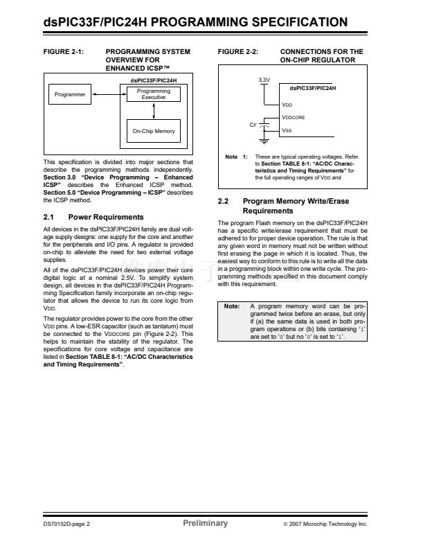
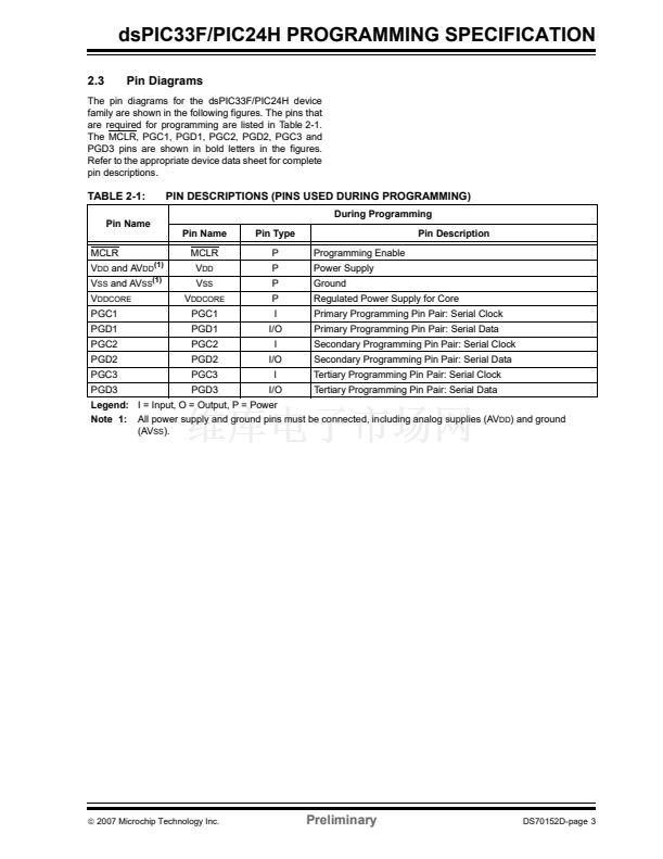
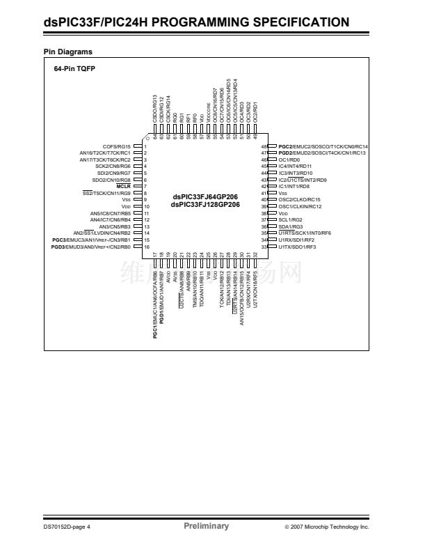
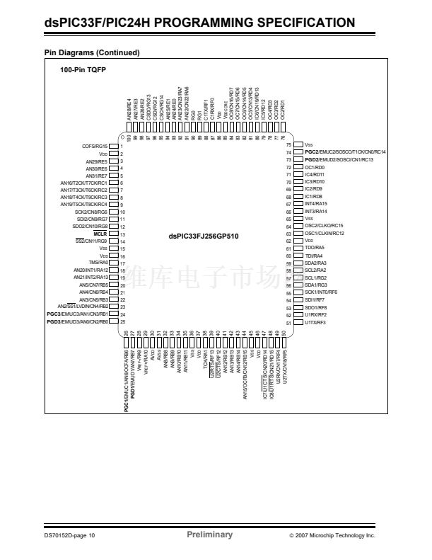
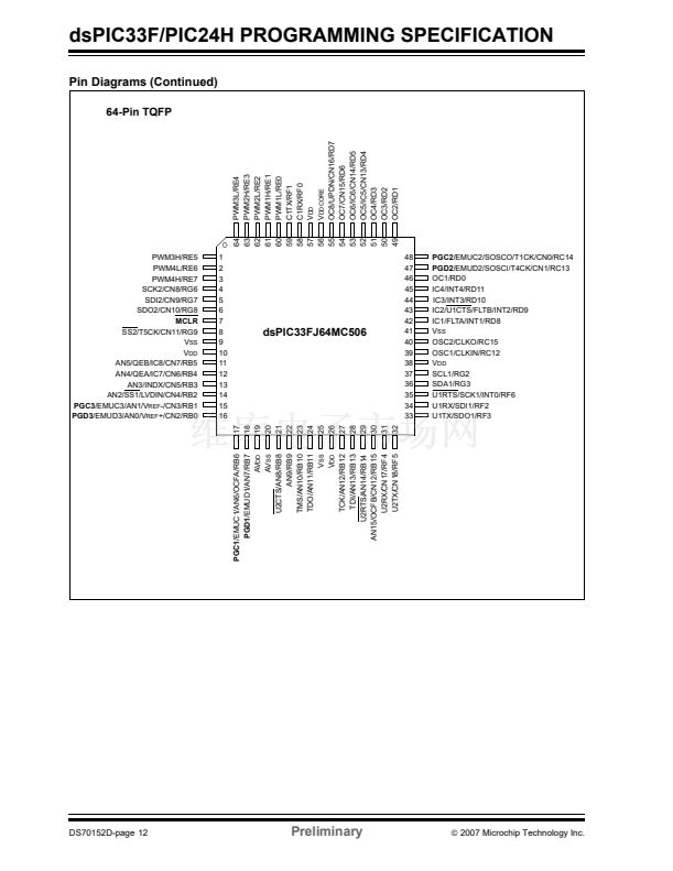
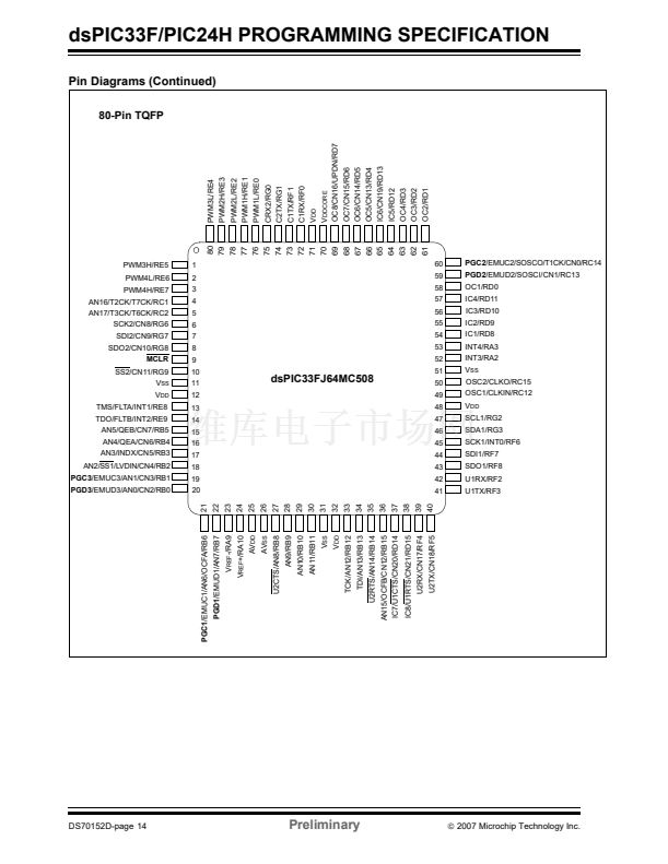
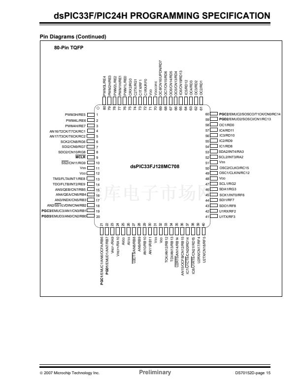
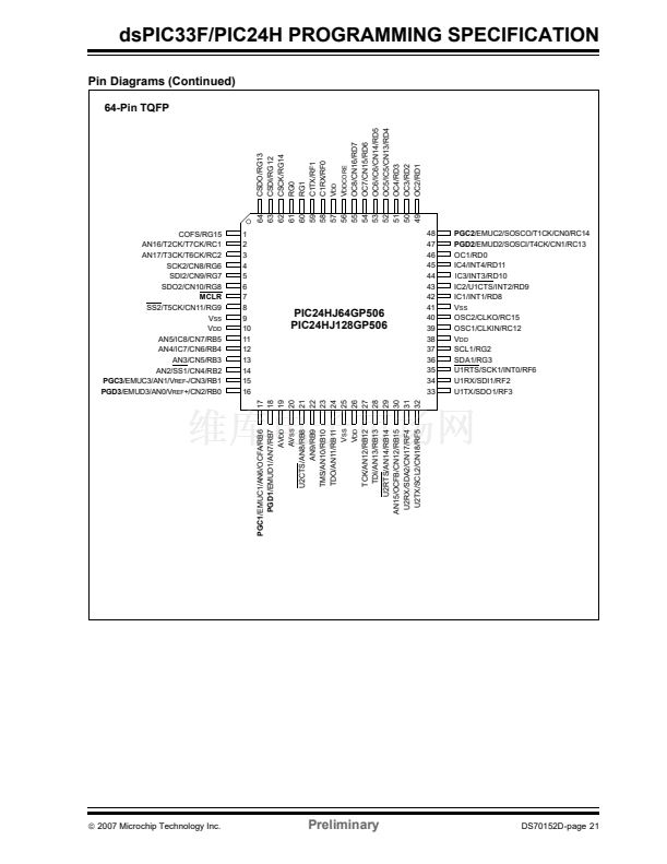
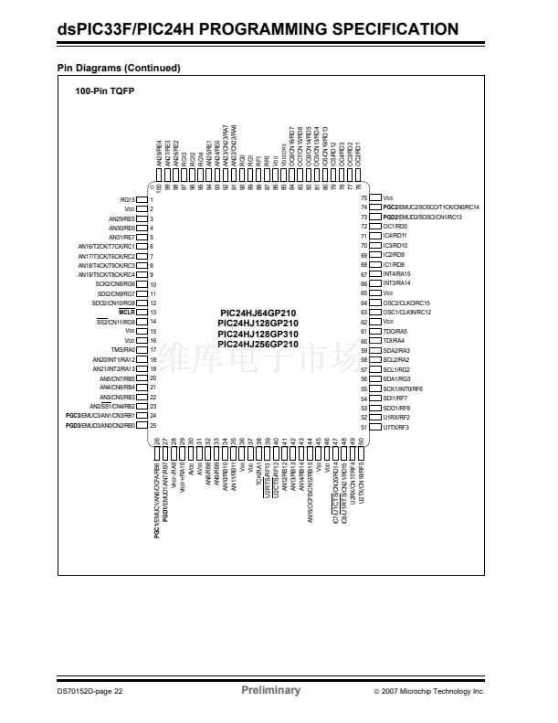
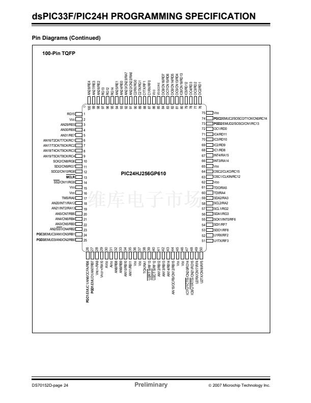
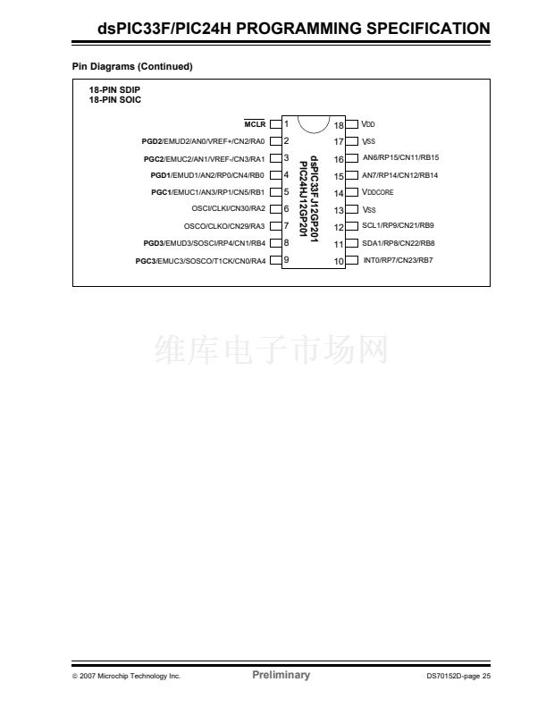
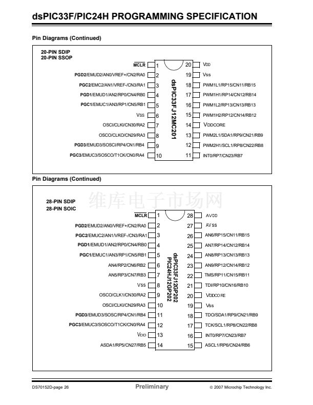
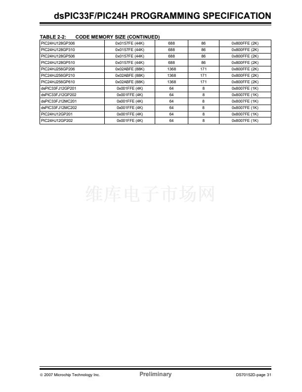
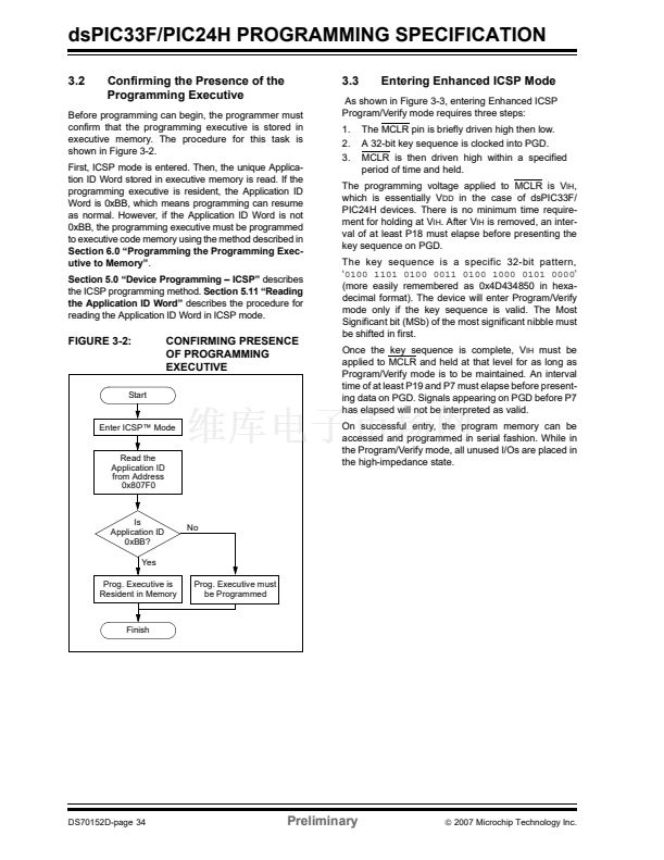
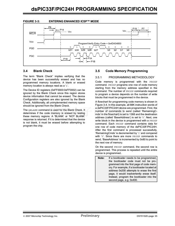
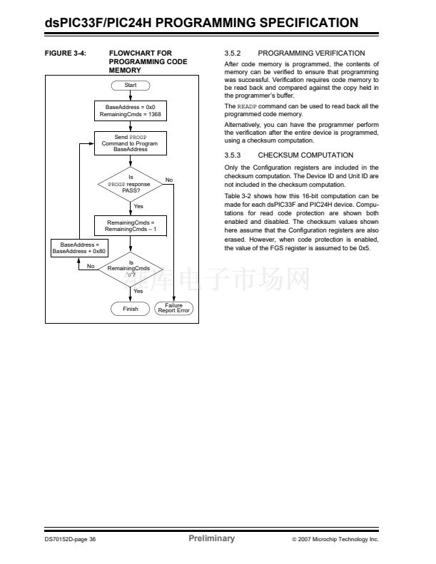
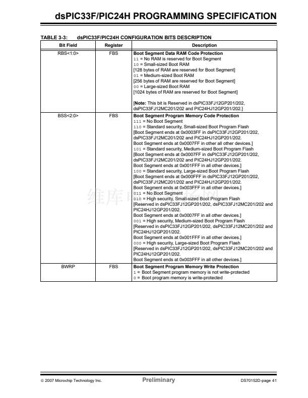
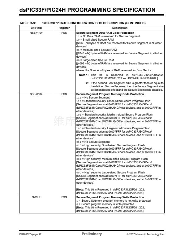
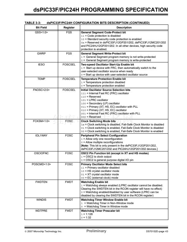
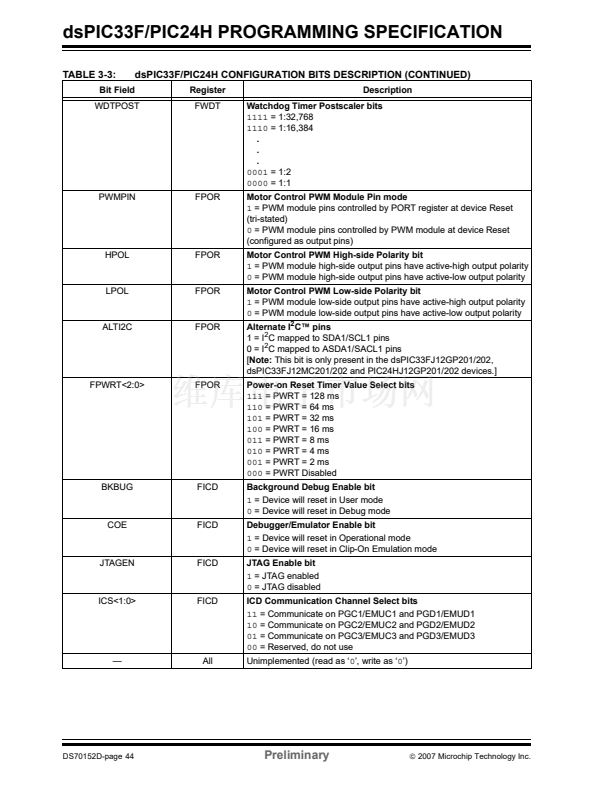
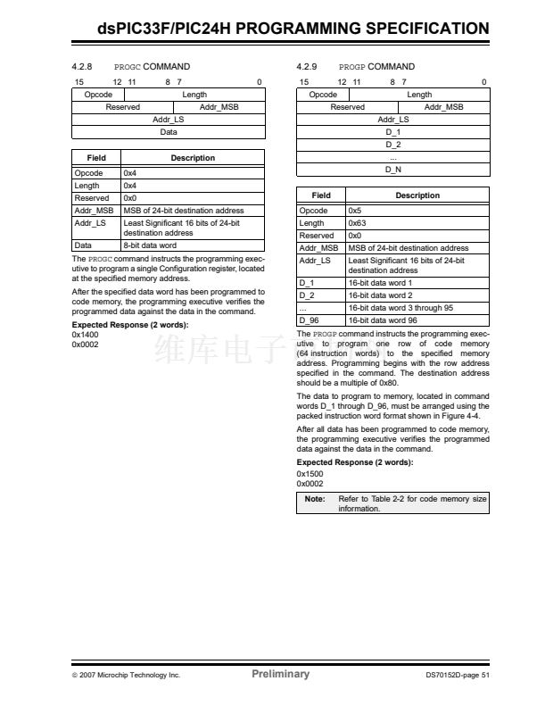
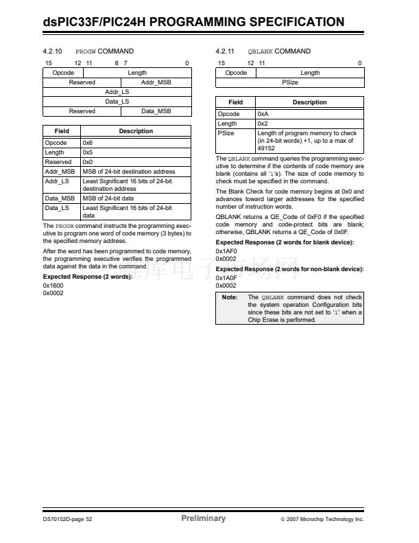
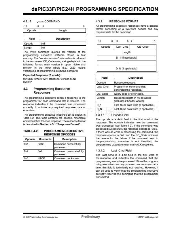
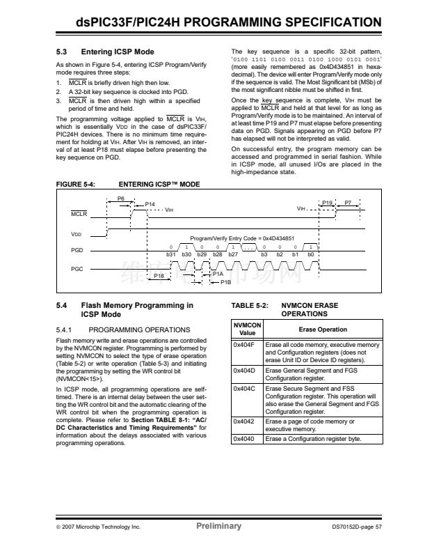
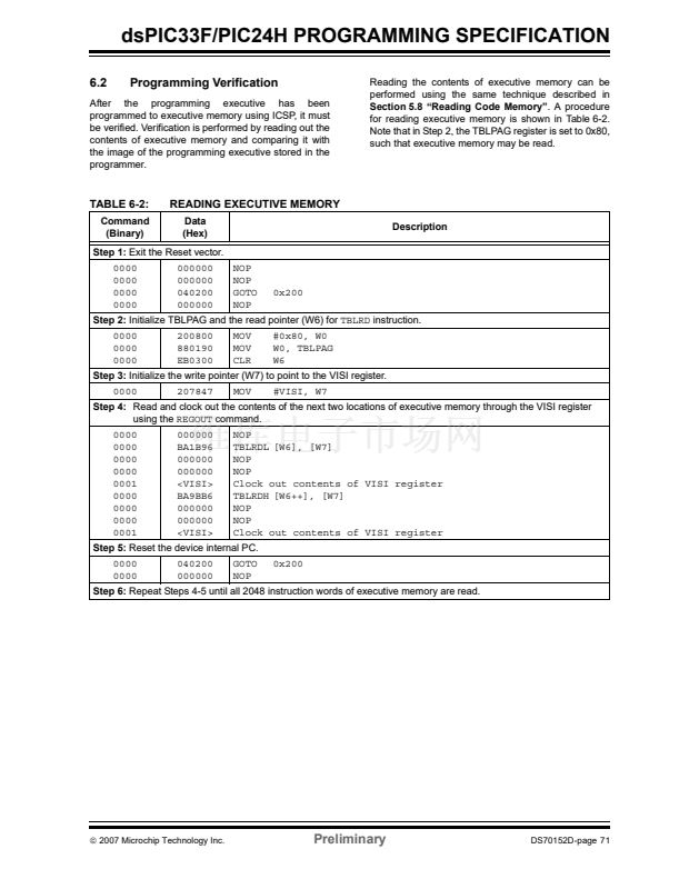
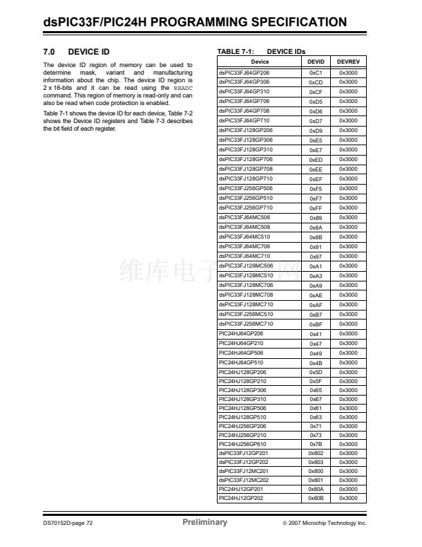
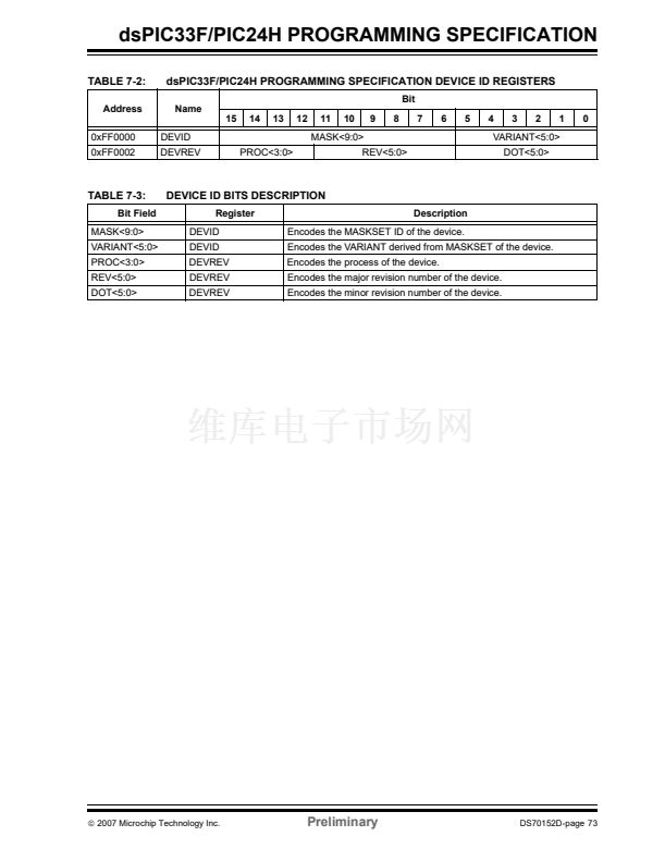
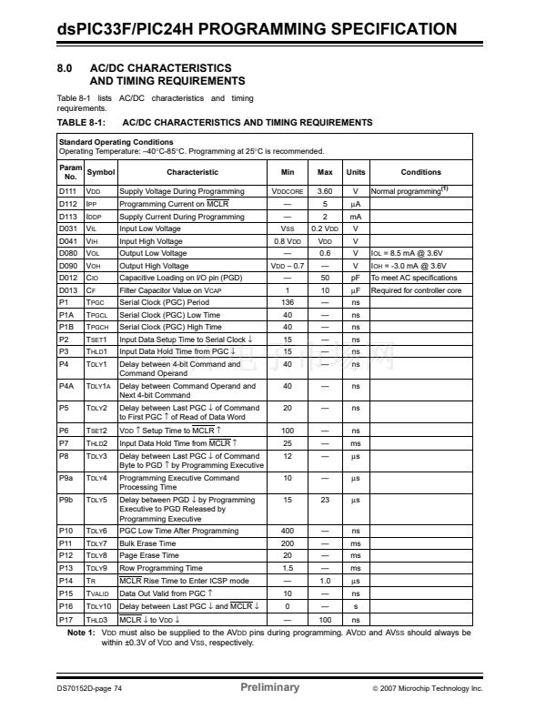
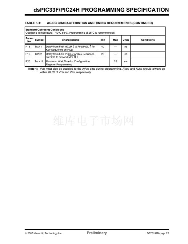
dsPIC33F/PIC24H PROGRAMMING SPECIFICATION
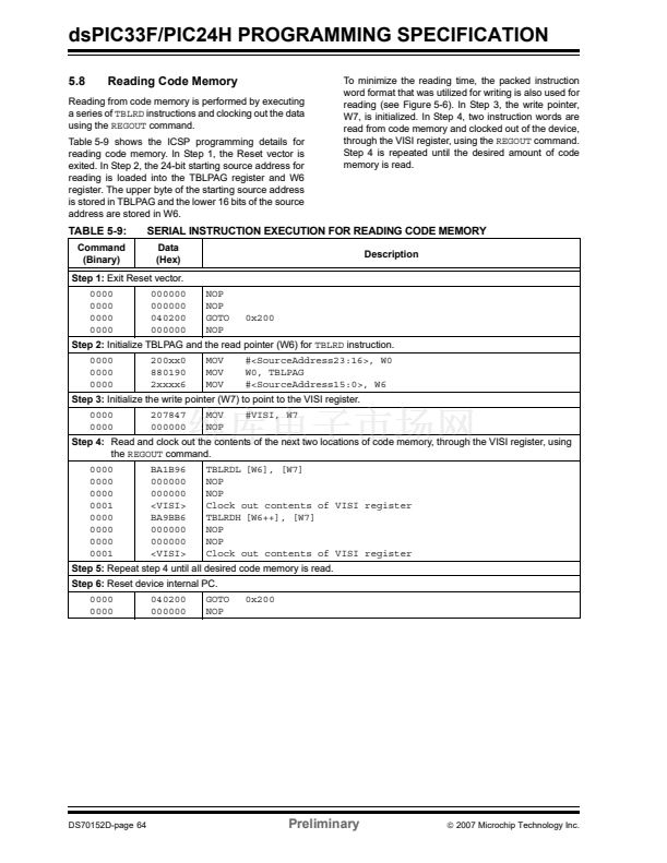
5.8
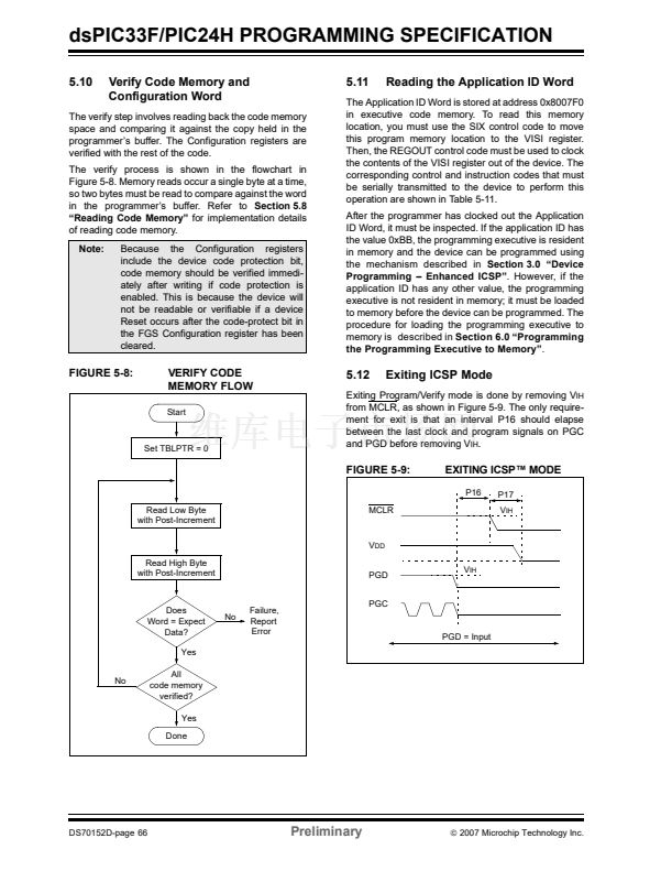
Reading Code Memory
To minimize the reading time, the packed instruction
word format that was utilized for writing is also used for
reading (see Figure 5-6). In Step 3, the write pointer,
W7, is initialized. In Step 4, two instruction words are
read from code memory and clocked out of the device,
through the VISI register, using the
REGOUT
command.
Step 4 is repeated until the desired amount of code
memory is read.
Reading from code memory is performed by executing
a series of
TBLRD
instructions and clocking out the data
using the
REGOUT
command.
Table 5-9 shows the ICSP programming details for
reading code memory. In Step 1, the Reset vector is
exited. In Step 2, the 24-bit starting source address for
reading is loaded into the TBLPAG register and W6
register. The upper byte of the starting source address
is stored in TBLPAG and the lower 16 bits of the source
address are stored in W6.
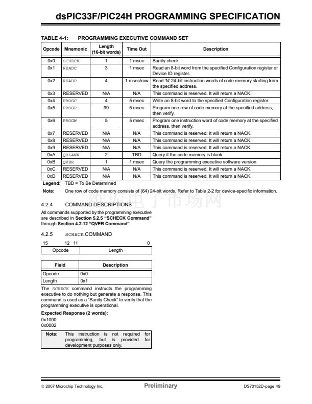
TABLE 5-9:
Command
(Binary)
SERIAL INSTRUCTION EXECUTION FOR READING CODE MEMORY
Data
(Hex)
Description
Step 1:
Exit Reset vector.
0000
0000
0000
0000
0000
0000
0000
0000
0000
000000
000000
040200
000000
200xx0
880190
2xxxx6
207847
000000
NOP
NOP
GOTO
NOP
MOV
MOV
MOV
MOV
NOP
0x200
Step 2:
Initialize TBLPAG and the read pointer (W6) for
TBLRD
instruction.
#<SourceAddress23:16>, W0
W0, TBLPAG
#<SourceAddress15:0>, W6
#VISI, W7
Step 3:
Initialize the write pointer (W7) to point to the VISI register.
Step 4:
Read and clock out the contents of the next two locations of code memory, through the VISI register, using
the
REGOUT
command.
0000
0000
0000
0001
0000
0000
0000
0001
BA1B96
000000
000000
<VISI>
BA9BB6
000000
000000
<VISI>
TBLRDL [W6], [W7]
NOP
NOP
Clock out contents of VISI register
TBLRDH [W6++], [W7]
NOP
NOP
Clock out contents of VISI register
Step 5:
Repeat step 4 until all desired code memory is read.
Step 6:
Reset device internal PC.
0000
0000
040200
000000
GOTO
NOP
0x200
DS70152D-page 64
Preliminary
漏
2007 Microchip Technology Inc.


 1
1
 2
2
 3
3
 4
4
 5
5
 6
6
 7
7
 8
8
 9
9
 10
10
 11
11
 12
12
 13
13
 14
14
 15
15
 16
16
 17
17
 18
18
 19
19
 20
20
 21
21
 22
22
 23
23
 24
24
 25
25
 26
26
 27
27
 28
28
 29
29
 30
30
 31
31
 32
32
 33
33
 34
34
 35
35
 36
36
 37
37
 38
38
 39
39
 40
40
 41
41
 42
42
 43
43
 44
44
 45
45
 46
46
 47
47
 48
48
 49
49
 50
50
 51
51
 52
52
 53
53
 54
54
 55
55
 56
56
 57
57
 58
58
 59
59
 60
60
 61
61
 62
62
 63
63
 64
64
 65
65
 66
66
 67
67
 68
68
 69
69
 70
70
 71
71
 72
72
 73
73
 74
74
 75
75
 76
76
 77
77
 78
78
 79
79
 80
80
