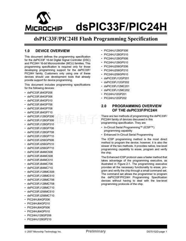
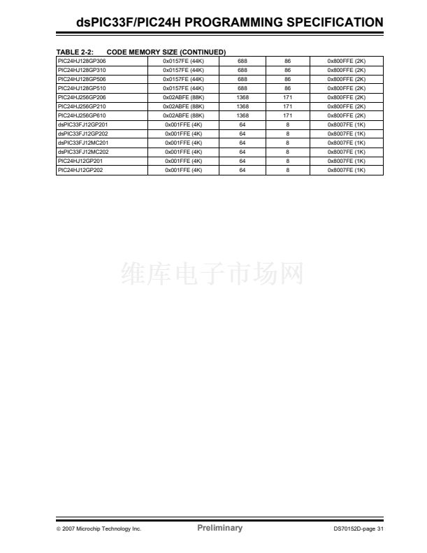
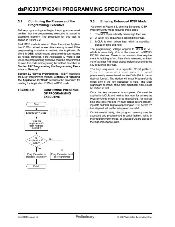
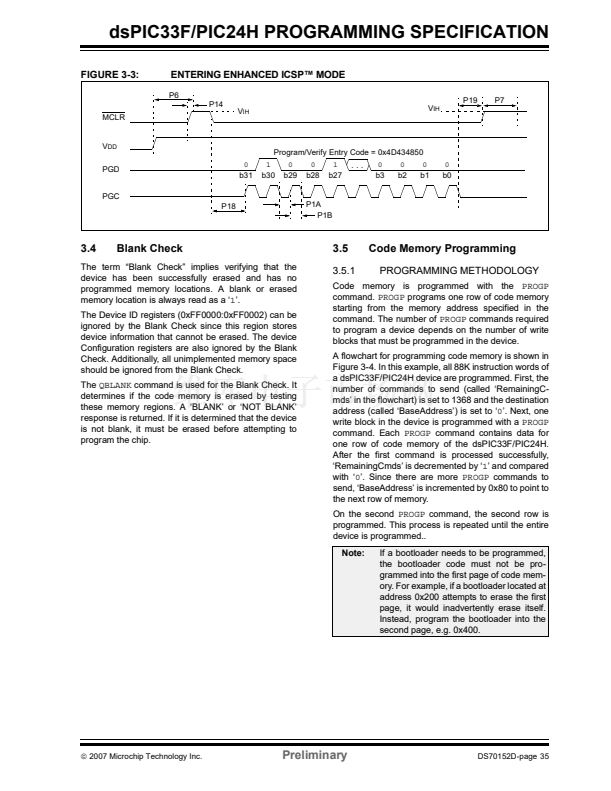
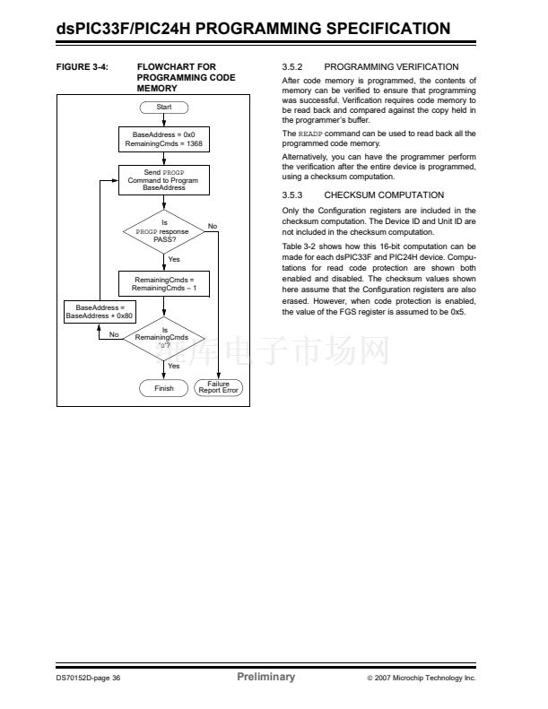
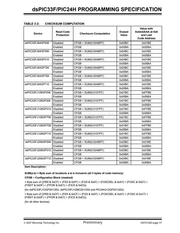
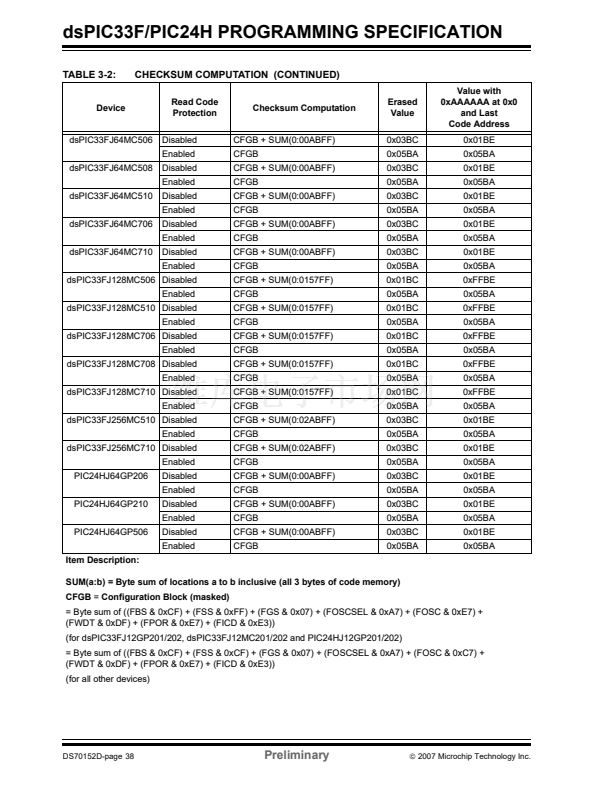
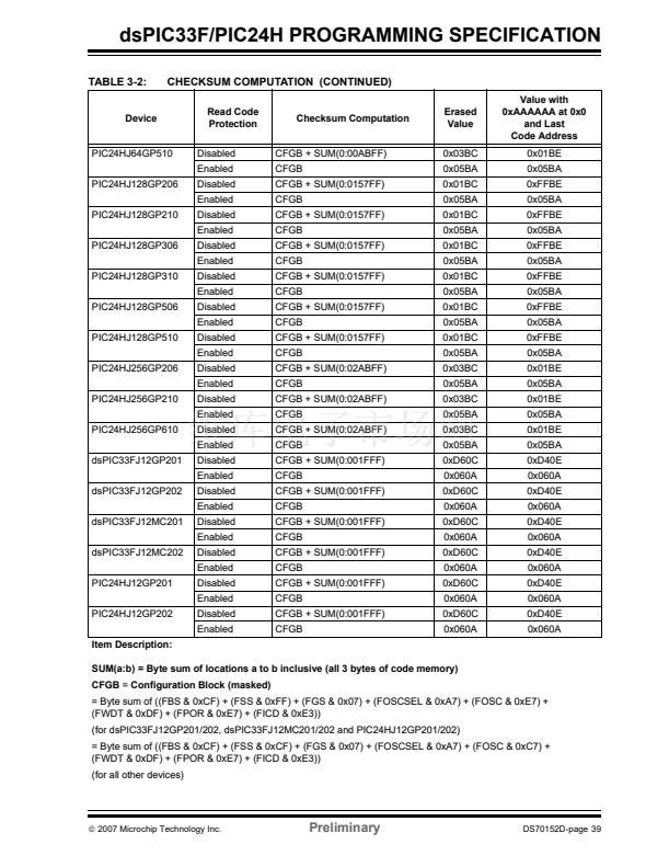
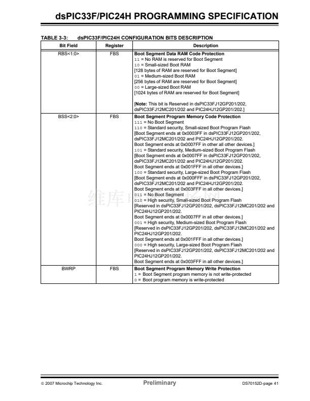
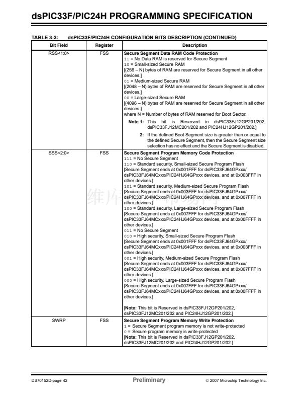
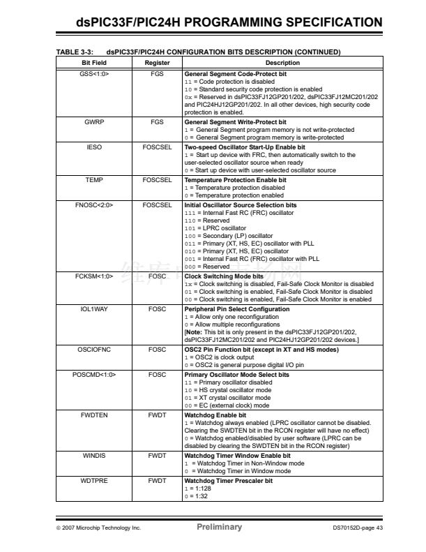
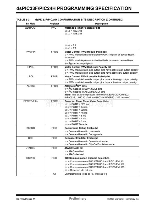
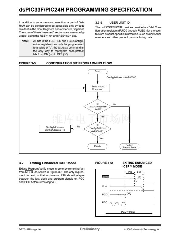
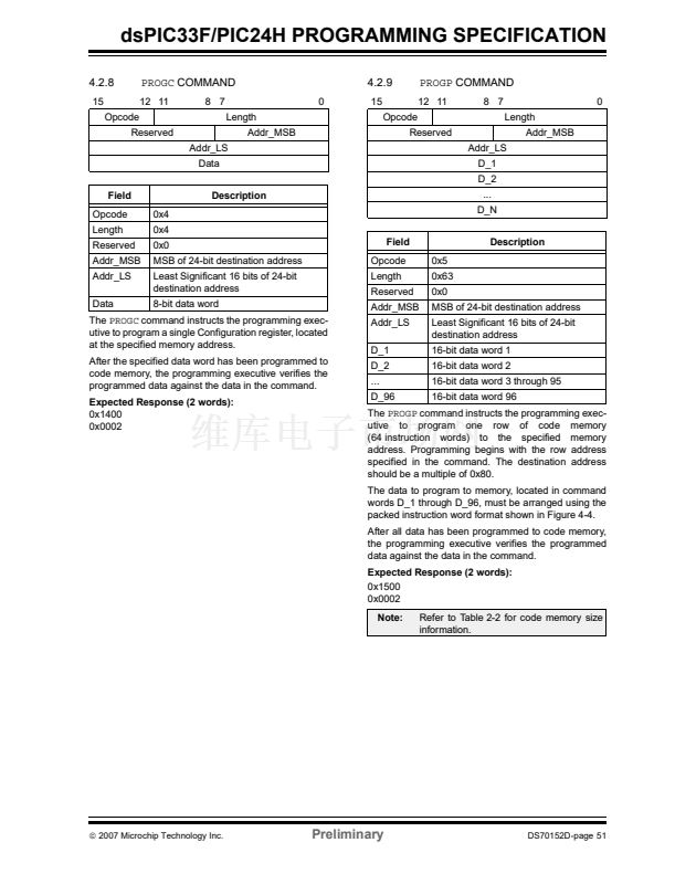
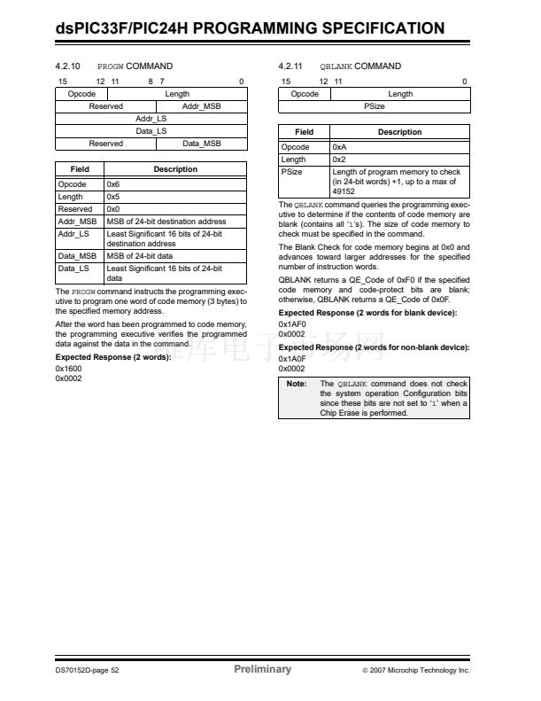
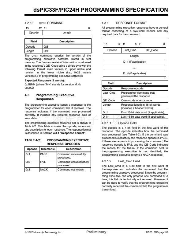
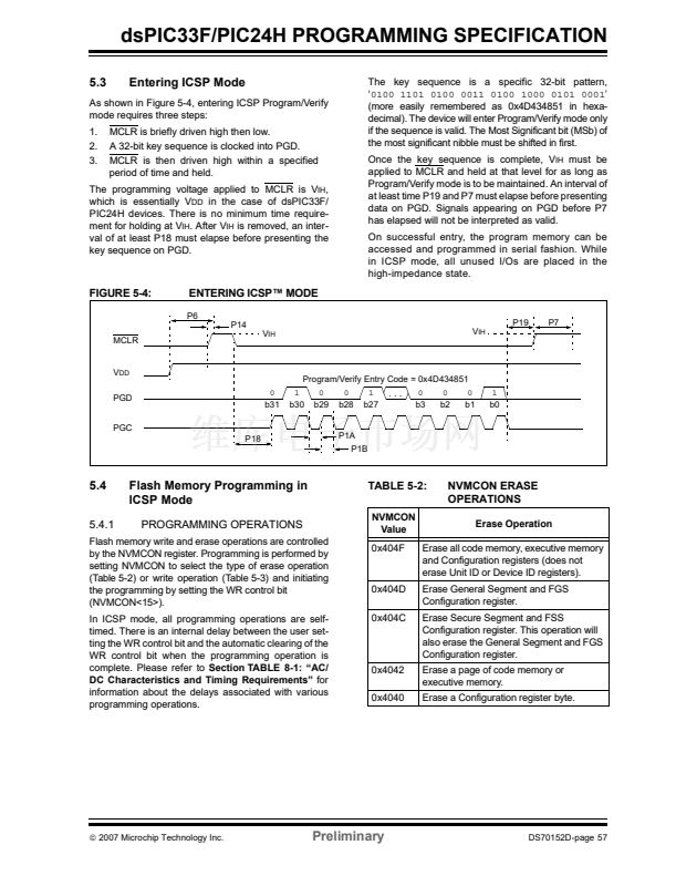
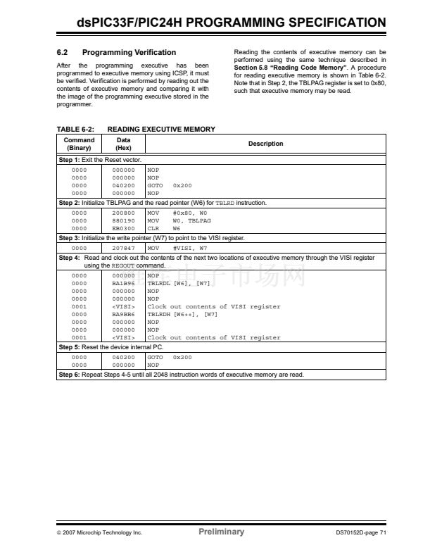
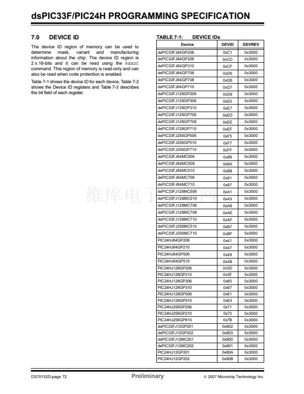
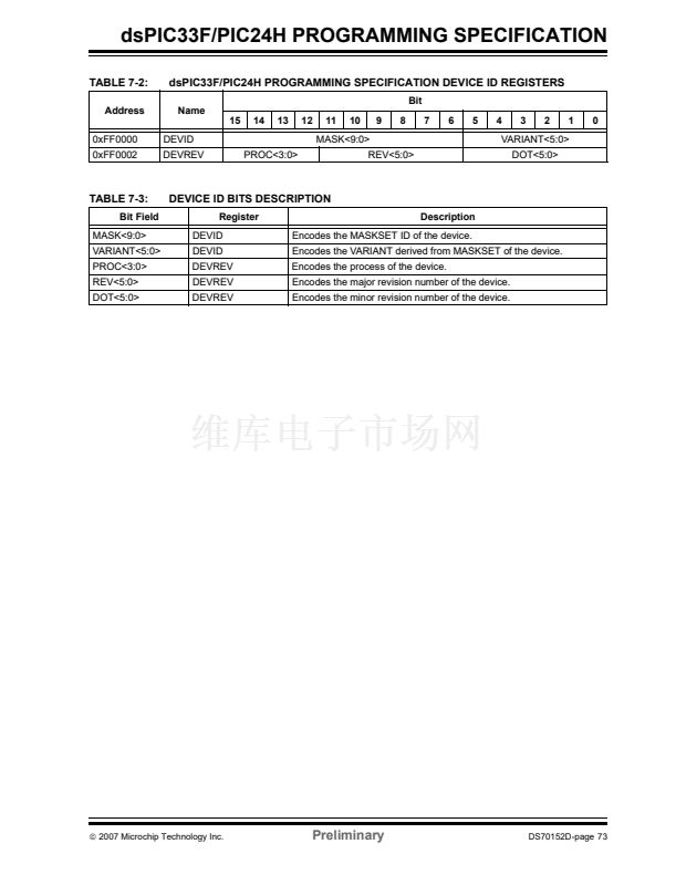
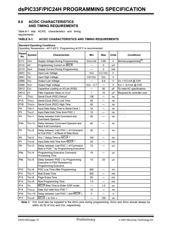
dsPIC33F/PIC24H PROGRAMMING SPECIFICATION
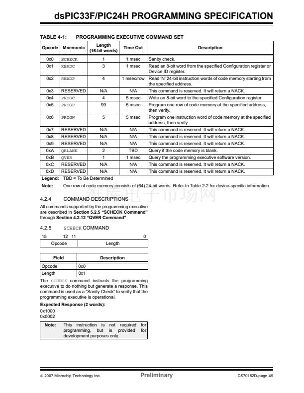
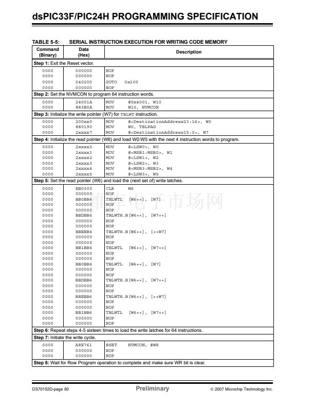
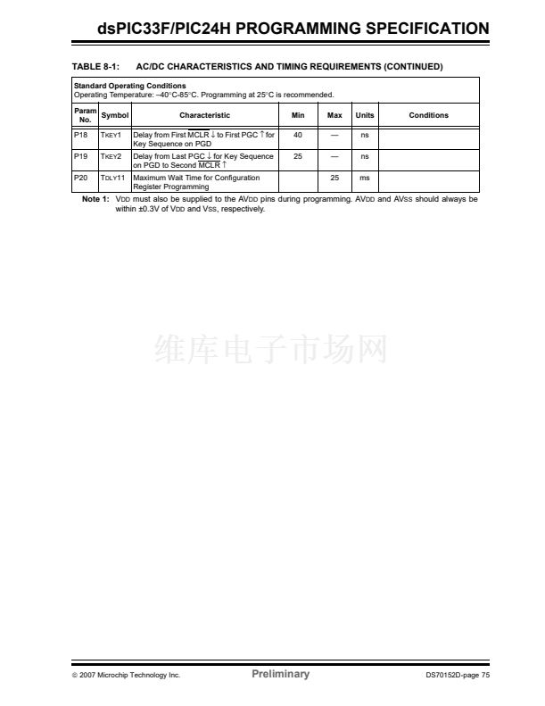
TABLE 5-5:
Command
(Binary)
-
SERIAL INSTRUCTION EXECUTION FOR WRITING CODE MEMORY (CONTINUED)
Data
(Hex)
-
Description
Externally time 鈥楶13鈥?msec (see
Section TABLE 8-1: 鈥淎C/DC
Characteristics and Timing Requirements鈥?
to allow suffi-
cient time for the Row Program operation to complete.
MOV
NVMCON, W0
MOV
W0, VISI
NOP
Clock out contents of VISI register. Repeat until the WR bit
is clear.
GOTO
NOP
0x200
0000
0000
0000
0001
807600
887840
000000
<VISI>
Step 9:
Reset device internal PC.
0000
0000
040200
000000
Step 10:
Repeat steps 3-9 until all code memory is programmed.
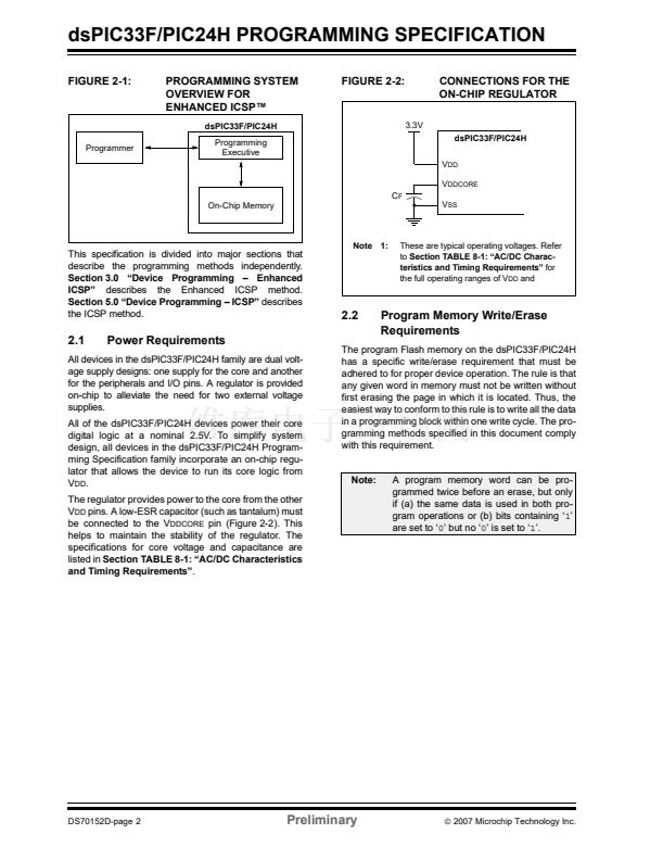
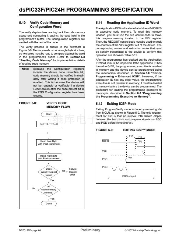
FIGURE 5-7:
PROGRAM CODE MEMORY FLOW
Start
N=1
LoopCount = 0
Configure
Device for
Writes
N=N+1
Load 2 Bytes
to Write
Buffer at <Addr>
No
All
bytes
written?
Yes
Start Write Sequence
and Poll for WR bit
to be cleared
N=1
LoopCount =
LoopCount + 1
No
All
locations
done?
Yes
Done
漏
2007 Microchip Technology Inc.
Preliminary
DS70152D-page 61


 1
1
 2
2
 3
3
 4
4
 5
5
 6
6
 7
7
 8
8
 9
9
 10
10
 11
11
 12
12
 13
13
 14
14
 15
15
 16
16
 17
17
 18
18
 19
19
 20
20
 21
21
 22
22
 23
23
 24
24
 25
25
 26
26
 27
27
 28
28
 29
29
 30
30
 31
31
 32
32
 33
33
 34
34
 35
35
 36
36
 37
37
 38
38
 39
39
 40
40
 41
41
 42
42
 43
43
 44
44
 45
45
 46
46
 47
47
 48
48
 49
49
 50
50
 51
51
 52
52
 53
53
 54
54
 55
55
 56
56
 57
57
 58
58
 59
59
 60
60
 61
61
 62
62
 63
63
 64
64
 65
65
 66
66
 67
67
 68
68
 69
69
 70
70
 71
71
 72
72
 73
73
 74
74
 75
75
 76
76
 77
77
 78
78
 79
79
 80
80
