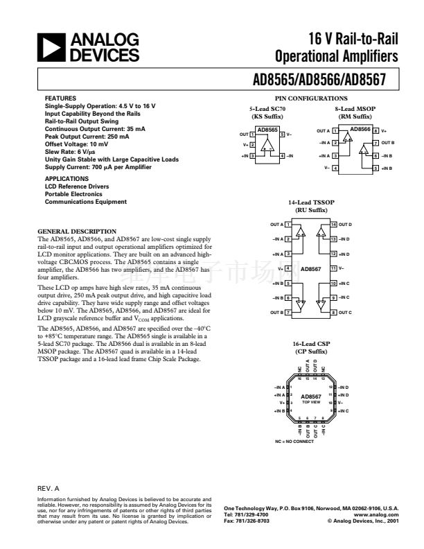
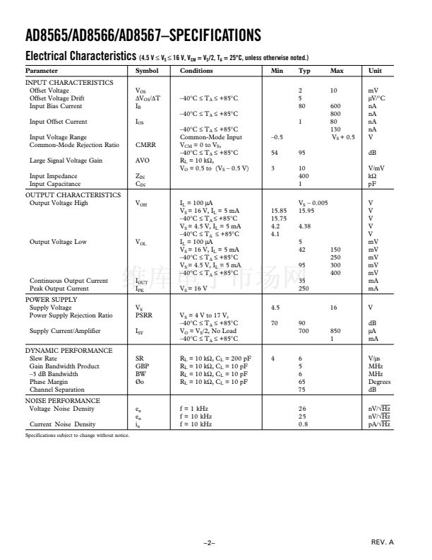
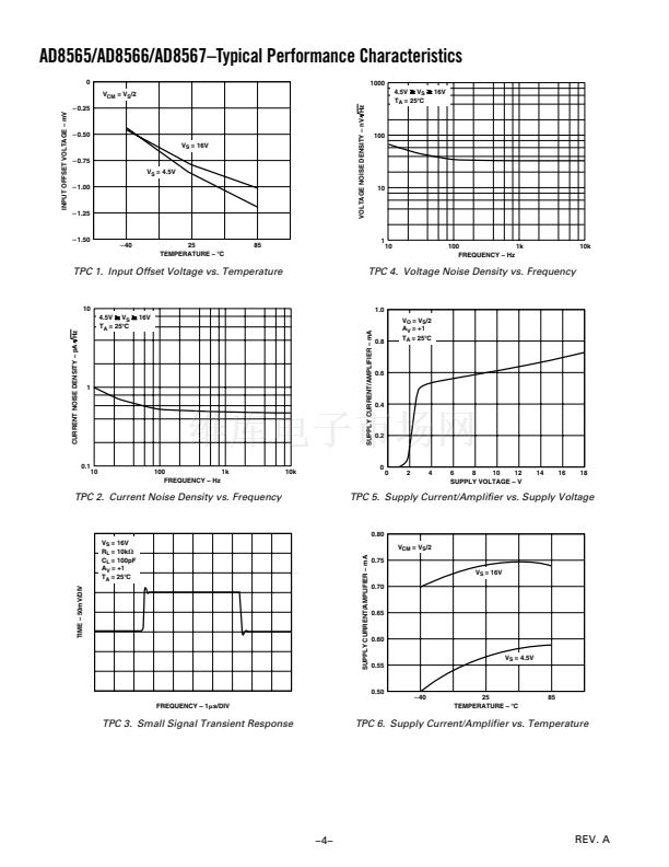
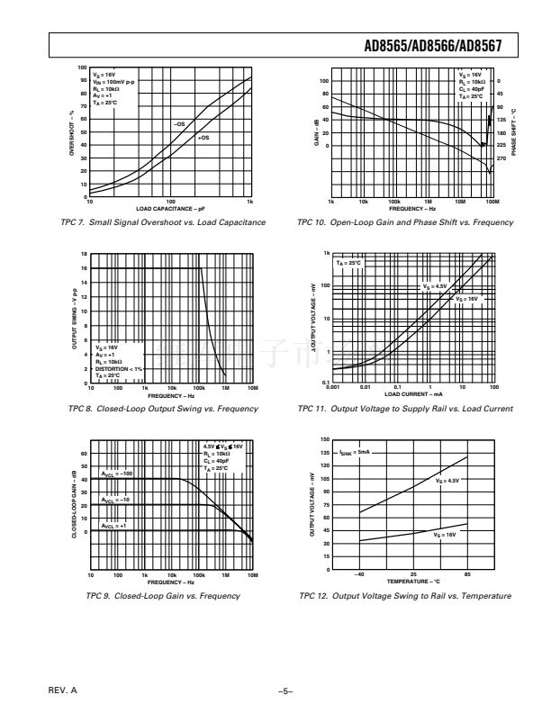
AD8565/AD8566/AD8567
APPLICATIONS
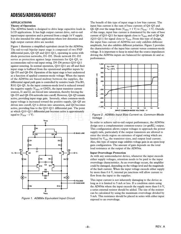
Theory of Operation
The AD856x family is designed to drive large capacitive loads in
LCD applications. It has high output current drive, rail-to-rail
input/output operation and is powered from a single 16 V supply.
It is also intended for other applications where low distortion and
high output current drive are needed.
Figure 1 illustrates a simplified equivalent circuit for the AD856x.
The rail-to-rail bipolar input stage is composed of two PNP
differential pairs, Q4鈥換5 and Q10鈥換11, operating in series with
diode protection networks, D1鈥揇2. Diode network D1鈥揇2
serves as protection against large transients for Q4鈥換5, to
accommodate rail-to-rail input swing. D5鈥揇6 protect Q10鈥換11
against zenering. In normal operation, Q10鈥換11 are off and their
input stage is buffered from the operational amplifier inputs by
Q6鈥揇3 and Q8鈥揇4. Operation of the input stage is best understood
as a function of applied common-mode voltage: When the inputs
of the AD856x are biased midway between the supplies, the
differential signal path gain is controlled by resistive loads (Via R9,
R10) Q4鈥換5. As the input common-mode level is reduced toward
the negative supply (V
NEG
or GND), the input transistor current
sources, I1 and I2, are forced into saturation, thereby forcing the
Q6鈥揇3 and Q8鈥揇4 networks into cutoff; However, Q4鈥換5 remain
active, providing input stage gain. Inversely, when common-mode
input voltage is increased toward the positive supply, Q4鈥換5 are
driven into cutoff, Q3 is driven into saturation, and Q4 becomes
active, providing bias to the Q10鈥換11 differential pair. The point
at which Q10鈥換11 differential pair becomes active is approximately
equal to (V
POS
鈥?1 V).
V
POS
The benefit of this type of input stage is low bias current. The
input bias current is the sum of base currents of Q4鈥換5 and
Q6鈥換8 over the range from (V
NEG
+ 1 V) to (V
POS
鈥?1 V). Outside
of this range, input bias current is dominated by the sum of base
current of Q10鈥換11 for input signals close to V
NEG
and of Q6鈥換8
(Q10鈥換11) for signal close to V
POS
. From this type of design,
the input bias current of AD856x not only exhibits different
amplitude, but also exhibits different polarities. Figure 2 provides
the characteristics of the input bias current versus common-mode
voltage. It is important to keep in mind that the source impedances
driving the AD856x inputs are balanced for optimum dc and ac
performance.
1,000
800
V
S
= 16V
T
A
= 25 C
INPUT BIAS CURRENT 鈥?nA
600
400
200
0
鈥?00
鈥?00
鈥?00
鈥?00
鈥?,000
0
2
4
6
8
10
12
INPUT COMMON-MODE VOLTAGE 鈥?V
14
16
Figure 2. AD856x Input Bias Current vs. Common-Mode
Voltage
R1
Q3
Q4
BIAS LINE
D1
R3
Q6
V+
C1
Q4
D3
R5
C2
D5
R6
D2
R4
Q8
Q5
D4
V鈥?/div>
In order to achieve rail-to-rail output performance, the AD856x
design uses a complementary common-source (or gmRL) output.
This configuration allows output voltages to approach the power
supply rails, particularly if the output transistors are allowed to
enter the triode region on extremes of signal swing which are
limited by V
GS
, the transistor sizes, and output load current.
Also, this type of output stage exhibits voltage gain in an open-loop
gain configuration. The amount of gain depends on the total
load resistance at the output of the AD856x.
Input Overvoltage Protection
Q10
Q11
I1
D6
I2
FOLDED
CASCADE
As with any semiconductor device, whenever the input exceeds
either supply voltages, attention needs to be paid to the input
overvoltage characteristics. As an overvoltage occurs, the amplifier
could be damaged, depending on the voltage level and the magnitude
of the fault current. When the input voltage exceeds either supply
by more than 0.6 V, internal pn junctions will allow current to
flow from the input to the supplies.
This input current is not inherently damaging to the device as
long as it is limited to 5 mA or less. If a condition exists using
the AD856x where the input exceeds the supply more than 0.6 V,
a series external resistor should be added. The size of the resistor
can be calculated by using the maximum overvoltage divided by
5 mA. This resistance should be placed in series with either input
exposed to an overvoltage.
R9
R10
V
NEG
Figure 1. AD856x Equivalent Input Circuit
prev
next


 1
1
 2
2
 3
3
 4
4
 5
5
 6
6
 7
7
 8
8
 9
9
 10
10
 11
11
 12
12
