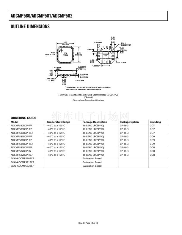
ADCMP580/ADCMP581/ADCMP582
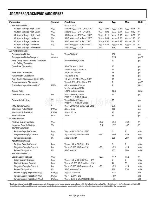
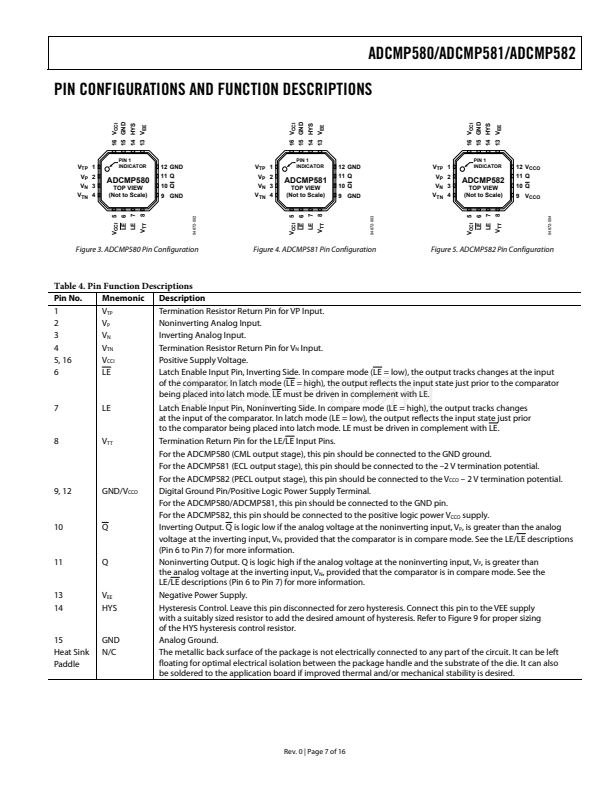
PIN CONFIGURATIONS AND FUNCTION DESCRIPTIONS
15 GND
15 GND
16 V
CCI
15 GND
16 V
CCI
16 V
CCI
14 HYS
14 HYS
13 V
EE
13 V
EE
14 HYS
13 V
EE
V
TP
1
V
P
2
V
N
3
V
TN
4
PIN 1
INDICATOR
12 GND
11 Q
10 Q
9 GND
V
TP
1
V
P
2
V
N
3
V
TN
4
PIN 1
INDICATOR
12 GND
11 Q
10 Q
9 GND
V
TP
1
V
P
2
V
N
3
V
TN
4
PIN 1
INDICATOR
12 V
CCO
11 Q
10 Q
9 V
CCO
ADCMP580
TOP VIEW
(Not to Scale)
ADCMP581
TOP VIEW
(Not to Scale)
ADCMP582
TOP VIEW
(Not to Scale)
V
TT
8
V
TT
8
V
CCI
5
V
CCI
5
V
CCI
5
04672-002
04672-003
V
TT
8
LE 7
LE 7
LE 7
LE
6
LE
6
LE
6
Figure 3. ADCMP580 Pin Configuration
Figure 4. ADCMP581 Pin Configuration
Figure 5. ADCMP582 Pin Configuration
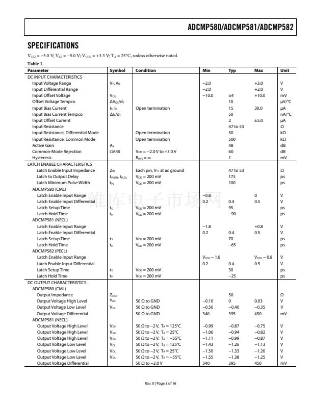
Table 4. Pin Function Descriptions
Pin No.
1
2
3
4
5, 16
6
Mnemonic
V
TP
V
P
V
N
V
TN
V
CCI
LE
Description
Termination Resistor Return Pin for VP Input.
Noninverting Analog Input.
Inverting Analog Input.
Termination Resistor Return Pin for V
N
Input.
Positive Supply Voltage.
Latch Enable Input Pin, Inverting Side. In compare mode (LE = low), the output tracks changes at the input
of the comparator. In latch mode (LE = high), the output reflects the input state just prior to the comparator
being placed into latch mode. LE must be driven in complement with LE.
Latch Enable Input Pin, Noninverting Side. In compare mode (LE = high), the output tracks changes
at the input of the comparator. In latch mode (LE = low), the output reflects the input state just prior
to the comparator being placed into latch mode. LE must be driven in complement with LE.
Termination Return Pin for the LE/LE Input Pins.
For the ADCMP580 (CML output stage), this pin should be connected to the GND ground.
For the ADCMP581 (ECL output stage), this pin should be connected to the 鈥? V termination potential.
For the ADCMP582 (PECL output stage), this pin should be connected to the V
CCO
鈥?2 V termination potential.
Digital Ground Pin/Positive Logic Power Supply Terminal.
For the ADCMP580/ADCMP581, this pin should be connected to the GND pin.
For the ADCMP582, this pin should be connected to the positive logic power V
CCO
supply.
Inverting Output. Q is logic low if the analog voltage at the noninverting input, V
P
, is greater than the analog
voltage at the inverting input, V
N
, provided that the comparator is in compare mode. See the LE/LE descriptions
(Pin 6 to Pin 7) for more information.
Noninverting Output. Q is logic high if the analog voltage at the noninverting input, V
P
, is greater than
the analog voltage at the inverting input, V
N
, provided that the comparator is in compare mode. See the
LE/LE descriptions (Pin 6 to Pin 7) for more information.
Negative Power Supply.
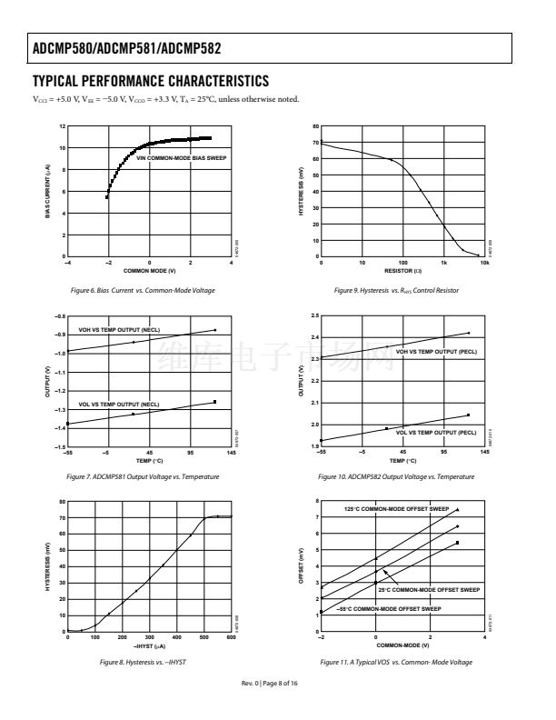
Hysteresis Control. Leave this pin disconnected for zero hysteresis. Connect this pin to the VEE supply
with a suitably sized resistor to add the desired amount of hysteresis. Refer to Figure 9 for proper sizing
of the HYS hysteresis control resistor.
Analog Ground.
The metallic back surface of the package is not electrically connected to any part of the circuit. It can be left
floating for optimal electrical isolation between the package handle and the substrate of the die. It can also
be soldered to the application board if improved thermal and/or mechanical stability is desired.
7
LE
8
V
TT
9, 12
GND/V
CCO
10
Q
11
Q
13
14
V
EE
HYS
15
Heat Sink
Paddle
GND
N/C
Rev. 0 | Page 7 of 16
04672-004


 1
1
 2
2
 3
3
 4
4
 5
5
 6
6
 7
7
 8
8
 9
9
 10
10
 11
11
 12
12
 13
13
 14
14
 15
15
 16
16
