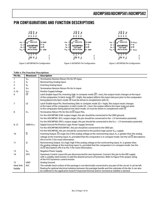
ADCMP580/ADCMP581/ADCMP582
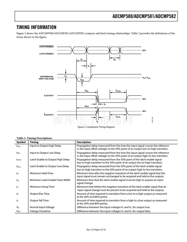
TIMING INFORMATION
Figure 2 shows the ADCMP580/ADCMP581/ADCMP582 compare and latch timing relationships. Table 2 provides the definitions of the
terms shown in the figure.
LATCH ENABLE
50%
LATCH ENABLE
t
S
t
H
t
PL
DIFFERENTIAL
INPUT VOLTAGE
V
N
V
OD
V
N
鹵 V
OS
t
PDL
Q OUTPUT
t
PLOH
50%
t
PDH
t
F
50%
Q OUTPUT
t
R
Figure 2. Comparator Timing Diagram
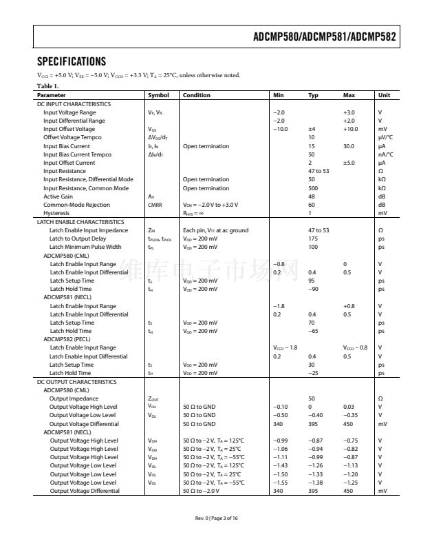
Table 2. Timing Descriptions
Symbol
t
PDH
t
PDL
t
PLOH
t
PLOL
t
H
t
PL
t
S
t
R
t
F
V
N
V
OD
Timing
Input to Output High Delay
Input to Output Low Delay
Latch Enable to Output High Delay
Latch Enable to Output Low Delay
Minimum Hold Time
Minimum Latch Enable Pulse Width
Minimum Setup Time
Output Rise Time
Output Fall Time
Normal Input Voltage
Voltage Overdrive
Description
Propagation delay measured from the time the input signal crosses the reference
(鹵 the input offset voltage) to the 50% point of an output low-to-high transition.
Propagation delay measured from the time the input signal crosses the reference
(鹵 the input offset voltage) to the 50% point of an output high-to-low transition.
Propagation delay measured from the 50% point of the latch enable signal
low-to-high transition to the 50% point of an output low-to-high transition.
Propagation delay measured from the 50% point of the latch enable signal
low-to-high transition to the 50% point of an output high-to-low transition.
Minimum time after the negative transition of the latch enable signal that the
input signal must remain unchanged to be acquired and held at the outputs.
Minimum time that the latch enable signal must be high to acquire an input
signal change.
Minimum time before the negative transition of the latch enable signal that an
input signal change must be present to be acquired and held at the outputs.
Amount of time required to transition from a low to a high output as measured
at the 20% and 80% points.
Amount of time required to transition from a high to a low output as measured
at the 20% and 80% points.
Difference between the input voltages V
P
and V
N
for output true.
Difference between the input voltages V
P
and V
N
for output false.
Rev. 0 | Page 5 of 16
04672-028
t
PLOL


 1
1
 2
2
 3
3
 4
4
 5
5
 6
6
 7
7
 8
8
 9
9
 10
10
 11
11
 12
12
 13
13
 14
14
 15
15
 16
16
