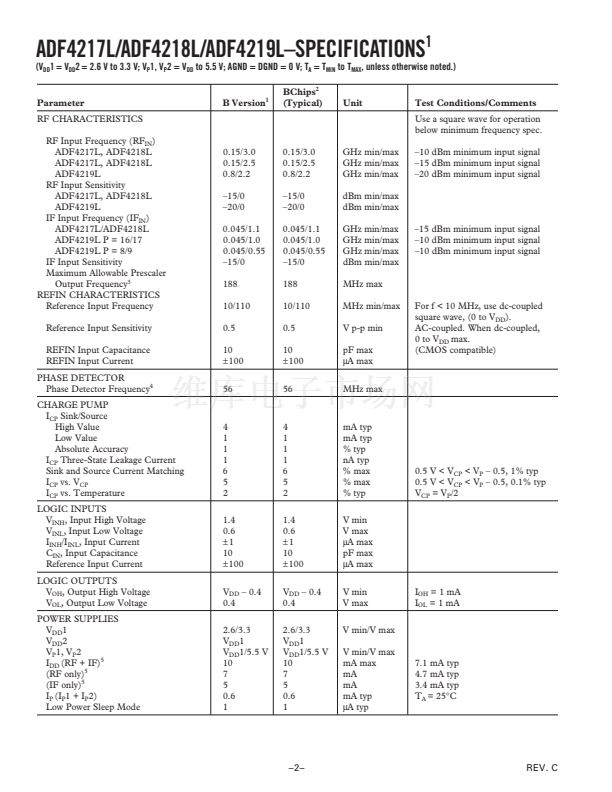
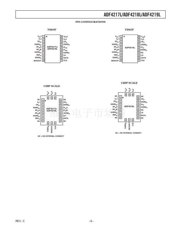
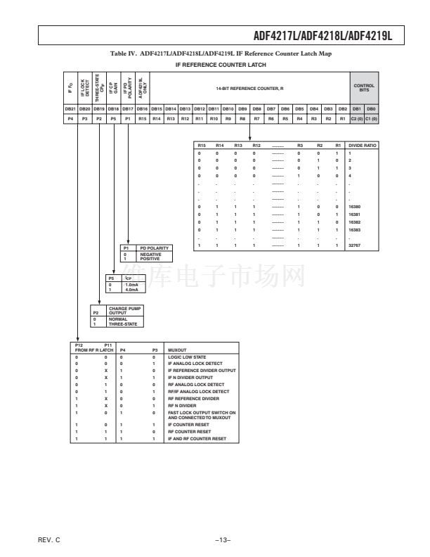
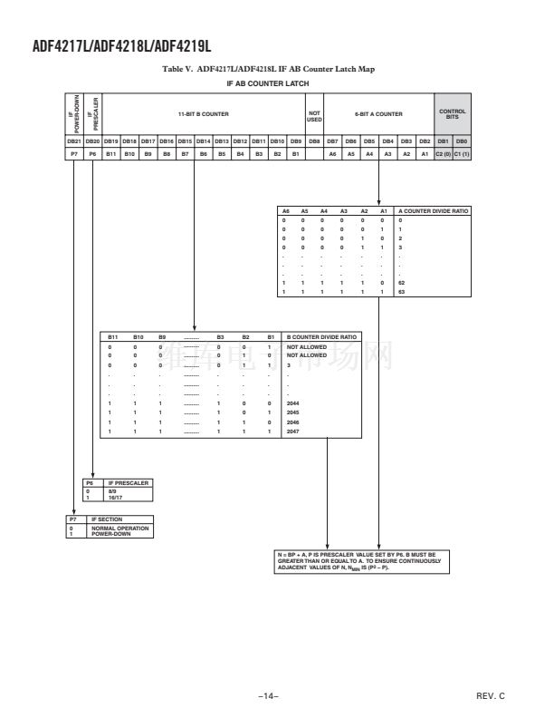
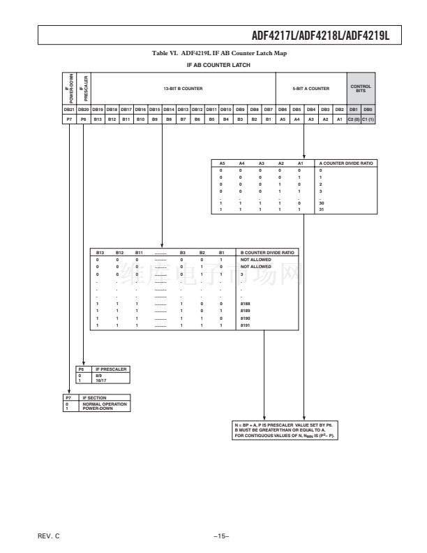
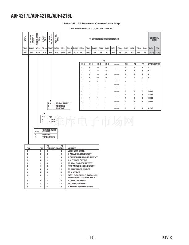
ADF4217L/ADF4218L/ADF4219L
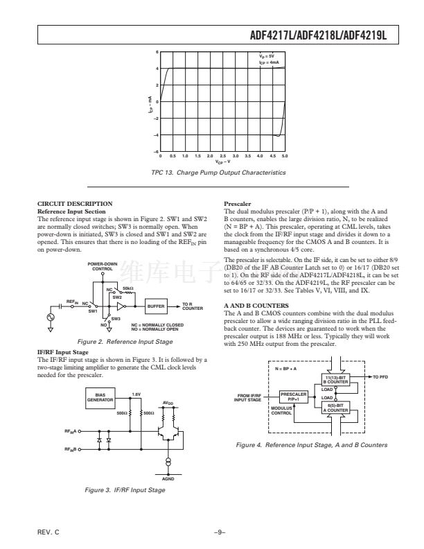
6
V
P
= 5V
I
CP
= 4mA
4
2
I
CP
鈥?mA
0
鈥?
鈥?
鈥?
0
0.5
1.0
1.5
2.0
2.5
3.0
V
CP
鈥?V
3.5
4.0
4.5
5.0
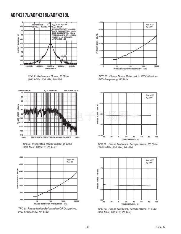
TPC 13. Charge Pump Output Characteristics
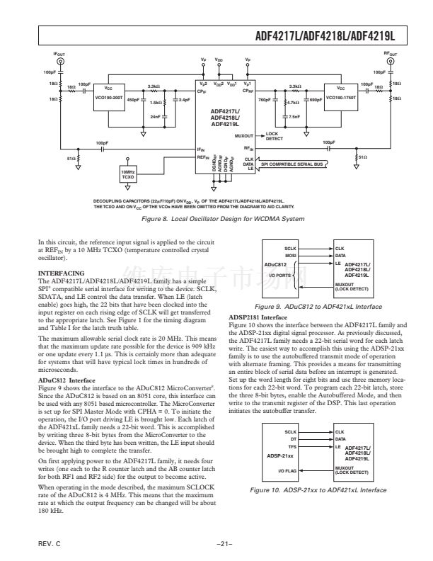
CIRCUIT DESCRIPTION
Reference Input Section
Prescaler
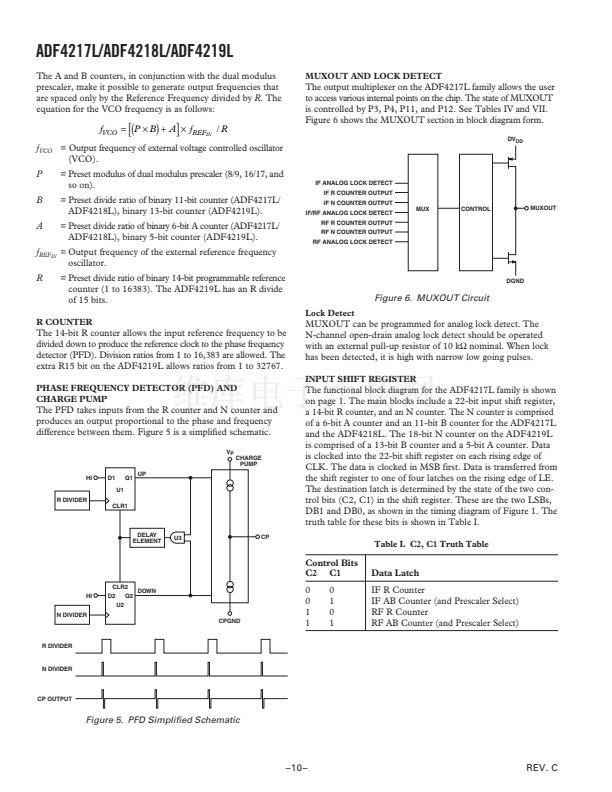
The reference input stage is shown in Figure 2. SW1 and SW2
are normally closed switches; SW3 is normally open. When
power-down is initiated, SW3 is closed and SW1 and SW2 are
opened. This ensures that there is no loading of the REF
IN
pin
on power-down.
POWER-DOWN
CONTROL
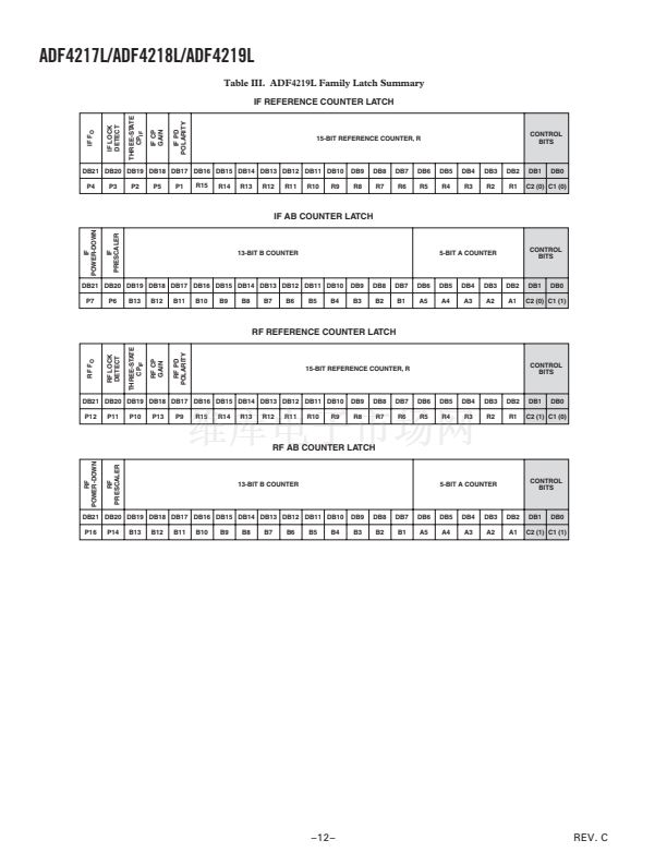
The dual modulus prescaler (P/P + 1), along with the A and
B counters, enables the large division ratio, N, to be realized
(N = BP + A). This prescaler, operating at CML levels, takes
the clock from the IF/RF input stage and divides it down to a
manageable frequency for the CMOS A and B counters. It is
based on a synchronous 4/5 core.
The prescaler is selectable. On the IF side, it can be set to either 8/9
(DB20 of the IF AB Counter Latch set to 0) or 16/17 (DB20 set
to 1). On the RF side of the ADF4217L/ADF4218L, it can be set
to 64/65 or 32/33. On the ADF4219L, the RF prescaler can be
set to 16/17 or 32/33. See Tables V, VI, VIII, and IX.
NC
SW2
REF
IN
NC
SW1
SW3
NO
50k
BUFFER
TO R
COUNTER
A AND B COUNTERS
NC = NORMALLY CLOSED
NO = NORMALLY OPEN
Figure 2. Reference Input Stage
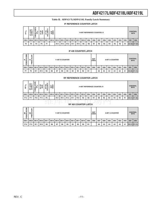
IF/RF Input Stage
The A and B CMOS counters combine with the dual modulus
prescaler to allow a wide ranging division ratio in the PLL feed-
back counter. The devices are guaranteed to work when the
prescaler output is 188 MHz or less. Typically they will work
with 250 MHz output from the prescaler.
The IF/RF input stage is shown in Figure 3. It is followed by a
two-stage limiting amplifier to generate the CML clock levels
needed for the prescaler.
BIAS
GENERATOR
500
1.6V
AV
DD
500
N = BP + A
11(13)-BIT
B COUNTER
LOAD
FROM IF/RF
INPUT STAGE
PRESCALER
P/P+1
MODULUS
CONTROL
LOAD
6(5)-BIT
A COUNTER
TO PFD
RF
IN
A
RF
IN
B
Figure 4. Reference Input Stage, A and B Counters
AGND
Figure 3. IF/RF Input Stage
REV. C
鈥?鈥?/div>
prev
next


 1
1
 2
2
 3
3
 4
4
 5
5
 6
6
 7
7
 8
8
 9
9
 10
10
 11
11
 12
12
 13
13
 14
14
 15
15
 16
16
 17
17
 18
18
 19
19
 20
20
 21
21
 22
22
 23
23
 24
24
