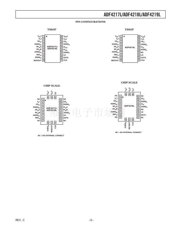
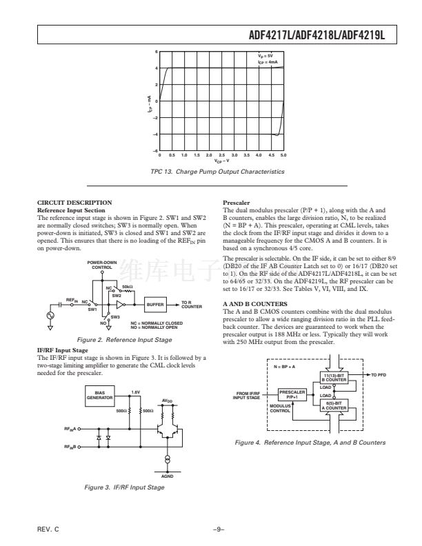
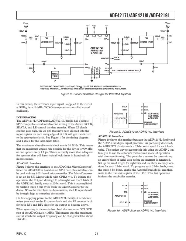
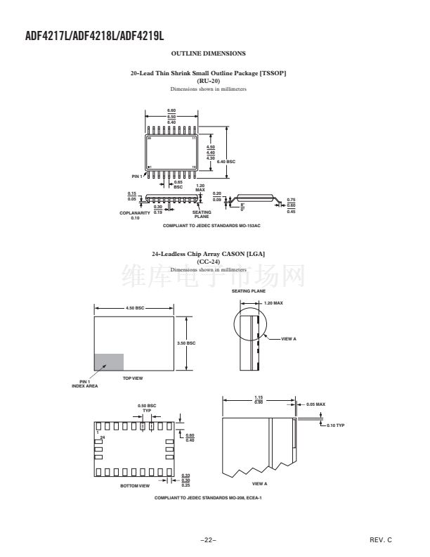
ADF4217L/ADF4218L/ADF4219L
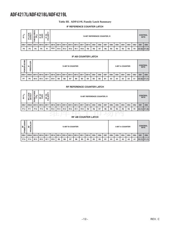
The A and B counters, in conjunction with the dual modulus
prescaler, make it possible to generate output frequencies that
are spaced only by the Reference Frequency divided by
R.
The
equation for the VCO frequency is as follows:
f
VCO
=
(
P
脳
B
)
+
A
脳
f
REF
IN
/
R
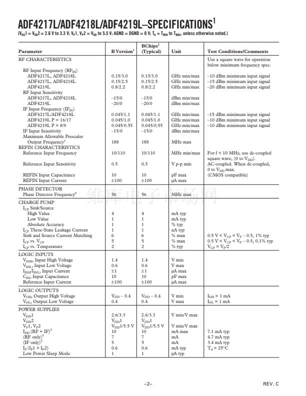
MUXOUT AND LOCK DETECT
[
]
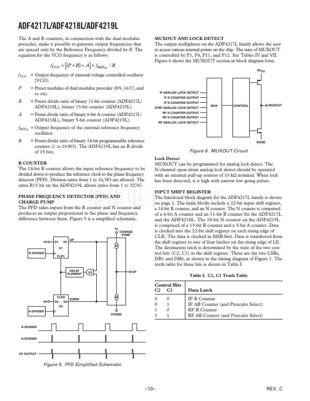
The output multiplexer on the ADF4217L family allows the user
to access various internal points on the chip. The state of MUXOUT
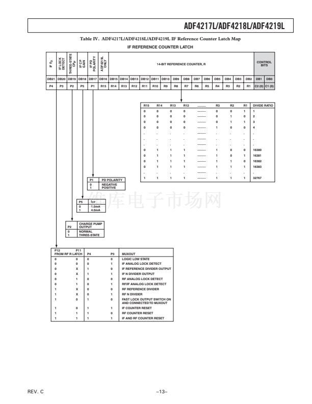
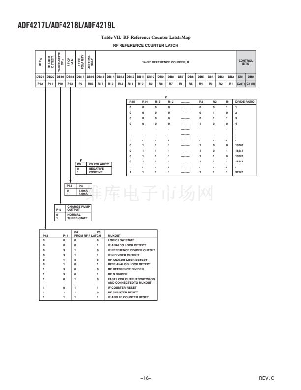
is controlled by P3, P4, P11, and P12. See Tables IV and VII.
Figure 6 shows the MUXOUT section in block diagram form.
DV
DD
f
VCO
= Output frequency of external voltage controlled oscillator
(VCO).
P
B
A
= Preset modulus of dual modulus prescaler (8/9, 16/17, and
so on).
= Preset divide ratio of binary 11-bit counter (ADF4217L/
ADF4218L), binary 13-bit counter (ADF4219L).
= Preset divide ratio of binary 6-bit A counter (ADF4217L/
ADF4218L), binary 5-bit counter (ADF4219L).
IF ANALOG LOCK DETECT
IF R COUNTER OUTPUT
IF N COUNTER OUTPUT
IF/RF ANALOG LOCK DETECT
RF R COUNTER OUTPUT
RF N COUNTER OUTPUT
RF ANALOG LOCK DETECT
MUX
CONTROL
MUXOUT
f
REF
IN
= Output frequency of the external reference frequency
oscillator.
R
= Preset divide ratio of binary 14-bit programmable reference
counter (1 to 16383). The ADF4219L has an R divide
of 15 bits.
Lock Detect
R COUNTER
DGND
Figure 6. MUXOUT Circuit
The 14-bit R counter allows the input reference frequency to be
divided down to produce the reference clock to the phase frequency
detector (PFD). Division ratios from 1 to 16,383 are allowed. The
extra R15 bit on the ADF4219L allows ratios from 1 to 32767.
PHASE FREQUENCY DETECTOR (PFD) AND
CHARGE PUMP
MUXOUT can be programmed for analog lock detect. The
N-channel open-drain analog lock detect should be operated
with an external pull-up resistor of 10 k鈩?nominal. When lock
has been detected, it is high with narrow low going pulses.
INPUT SHIFT REGISTER
The PFD takes inputs from the R counter and N counter and
produces an output proportional to the phase and frequency
difference between them. Figure 5 is a simpli鏗乪d schematic.
V
P
UP
CHARGE
PUMP
HI
D1
U1
Q1
R DIVIDER
CLR1
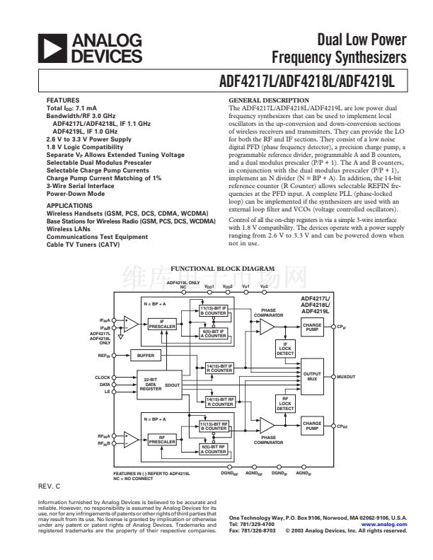
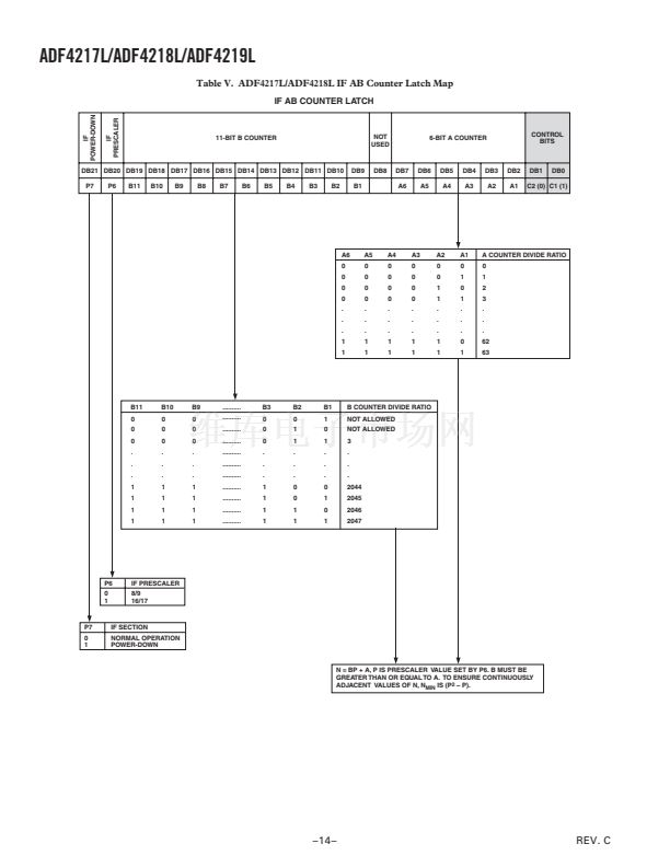
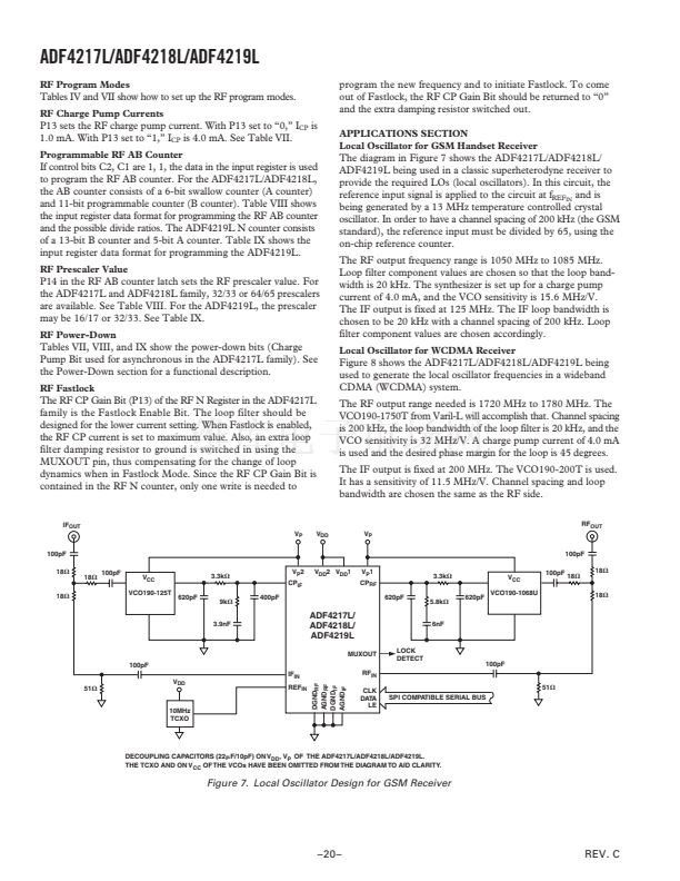
The functional block diagram for the ADF4217L family is shown
on page 1. The main blocks include a 22-bit input shift register,
a 14-bit R counter, and an N counter. The N counter is comprised
of a 6-bit A counter and an 11-bit B counter for the ADF4217L
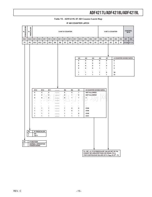
and the ADF4218L. The 18-bit N counter on the ADF4219L
is comprised of a 13-bit B counter and a 5-bit A counter. Data
is clocked into the 22-bit shift register on each rising edge of
CLK. The data is clocked in MSB first. Data is transferred from
the shift register to one of four latches on the rising edge of LE.
The destination latch is determined by the state of the two con-
trol bits (C2, C1) in the shift register. These are the two LSBs,
DB1 and DB0, as shown in the timing diagram of Figure 1. The
truth table for these bits is shown in Table I.
Table I. C2, C1 Truth Table
DELAY
ELEMENT
U3
CP
Control Bits
C2 C1
HI
N DIVIDER
CPGND
CLR2
DOWN
D2
Q2
U2
Data Latch
IF R Counter
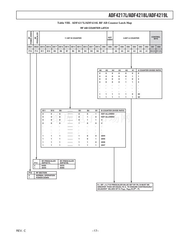
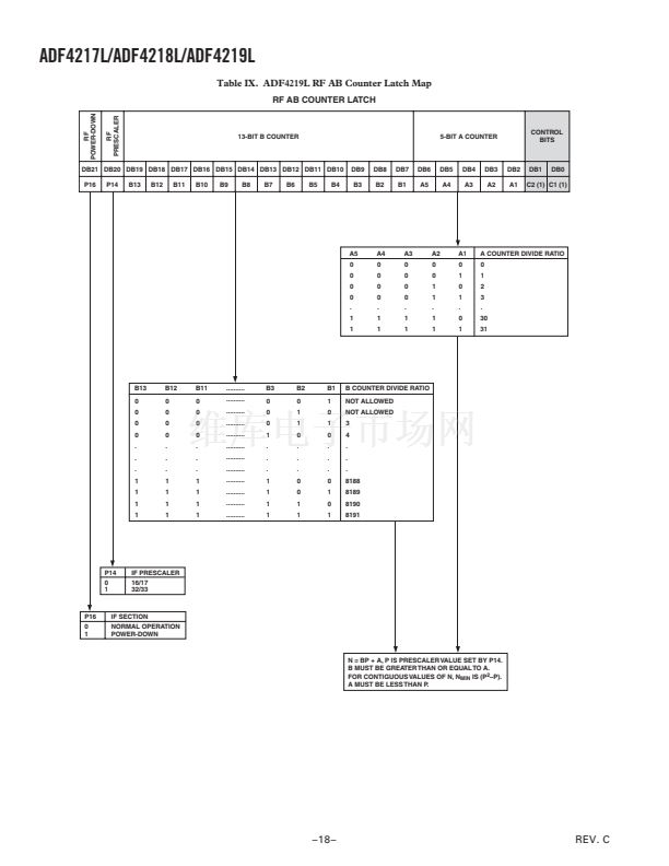
IF AB Counter (and Prescaler Select)
RF R Counter
RF AB Counter (and Prescaler Select)
0
0
1
1
0
1
0
1
R DIVIDER
N DIVIDER
CP OUTPUT
Figure 5. PFD Simplified Schematic
prev
next


 1
1
 2
2
 3
3
 4
4
 5
5
 6
6
 7
7
 8
8
 9
9
 10
10
 11
11
 12
12
 13
13
 14
14
 15
15
 16
16
 17
17
 18
18
 19
19
 20
20
 21
21
 22
22
 23
23
 24
24
