Preliminary Technical Data
Parameter
Min
0.8脳V
CC
0.8脳V
CC
RESET Output Voltage High
0.8脳V
CC
0.8脳V
CC
0.8脳V
CC
0.8脳V
CC
RESET Output Voltage Low
0.4
0.3
0.3
WATCHDOG INPUT (ADM6821-ADM6824)
Watchdog Timeout Period
WDI Pulse Width
WDI Input Threshold
V
IL
V
IH
WDI Input Current
MANUAL RESET INPUT (ADM6821-ADM6823/ADM6825)
MR Input Threshold
MR Input Pulse Width
MR Glitch Rejection
MR Pull-up Resistance
MR to Reset Delay
0.7xV
CC
1
25
100
50
200
75
V
V
V
Typ
Max
Units
V
V
ADM6821鈥揂DM6825
Test Conditions/Comments
V
CC
>=3.15V, I
SOURCE
=500uA,
reset not asserted
V
CC
>=1.8V, I
SOURCE
=200uA,
reset not asserted
V
CC
>=4.25V, I
SOURCE
=800uA,
reset asserted
V
CC
>=2.55V, I
SOURCE
=500uA,
reset asserted
V
CC
>=1.50V, I
SOURCE
=100uA,
reset asserted
V
CC
>=1.0V, I
SOURCE
=1uA,
reset asserted, T
A
=-40擄C to +85擄C
V
CC
>=4.75V, I
SINK
=3.2mA,
reset not asserted
V
CC
>=3.15V, I
SINK
=1.2mA,
reset not asserted
V
CC
>=1.8V, I
SINK
=500uA,
reset not asserted
1.12
50
1.6
2.40
s
ns
V
V
碌A(chǔ)
碌A(chǔ)
V
V
碌s
ns
k
ns
V
IL
=0.4V, V
IH
=0.8脳V
CC
,
0.3xV
CC
0.7xV
CC
-20
120
-15
160
V
WDI
= V
CC
, time average
V
WDI
=0, time average
0.3xV
CC
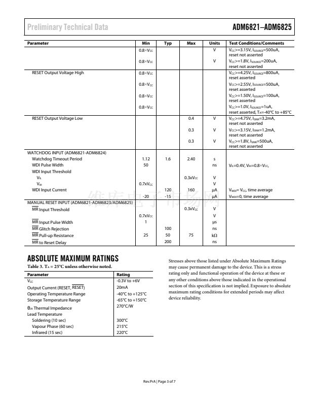
ABSOLUTE MAXIMUM RATINGS
Table 3. T
A
= 25擄C unless otherwise noted.
Parameter
V
CC
Output Current (RESET, RESET)
Operating Temperature Range
Storage Temperature Range
胃
JA
Thermal Impedance
Lead Temperature
Soldering (10 sec)
Vapour Phase (60 sec)
Infrared (15 sec)
Rating
-0.3V to +6V
20mA
-40擄C to +125擄C
-65擄C to +150擄C
270擄C/W
300擄C
215擄C
220擄C
Stresses above those listed under Absolute Maximum Ratings
may cause permanent damage to the device. This is a stress
rating only and functional operation of the device at these or
any other conditions above those indicated in the operational
section of this specification is not implied. Exposure to absolute
maximum rating conditions for extended periods may affect
device reliability.
Rev.PrA | Page 3 of 7


 1
1
 2
2
 3
3
 4
4
 5
5
 6
6
 7
7
