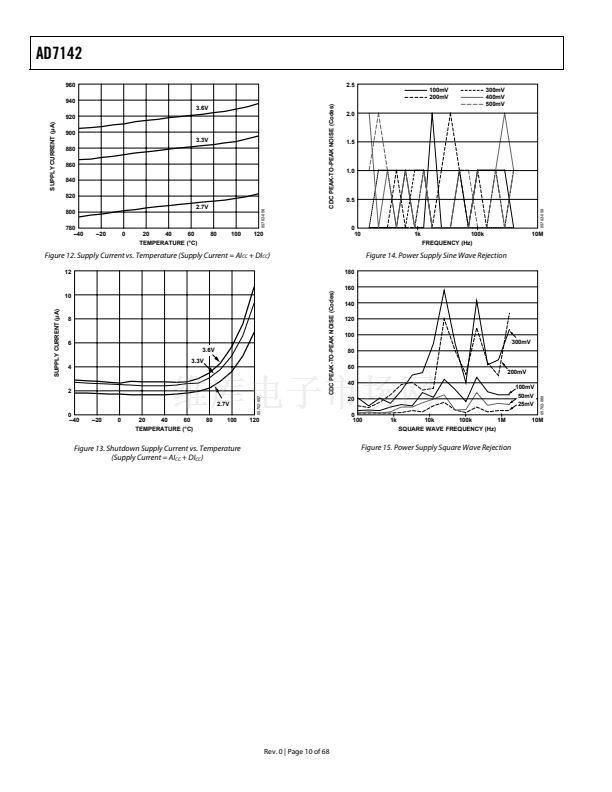
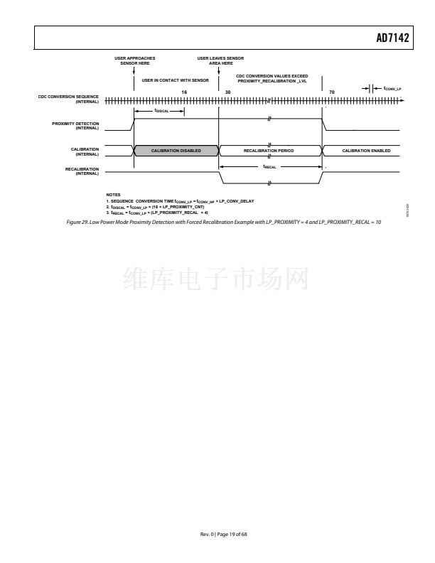
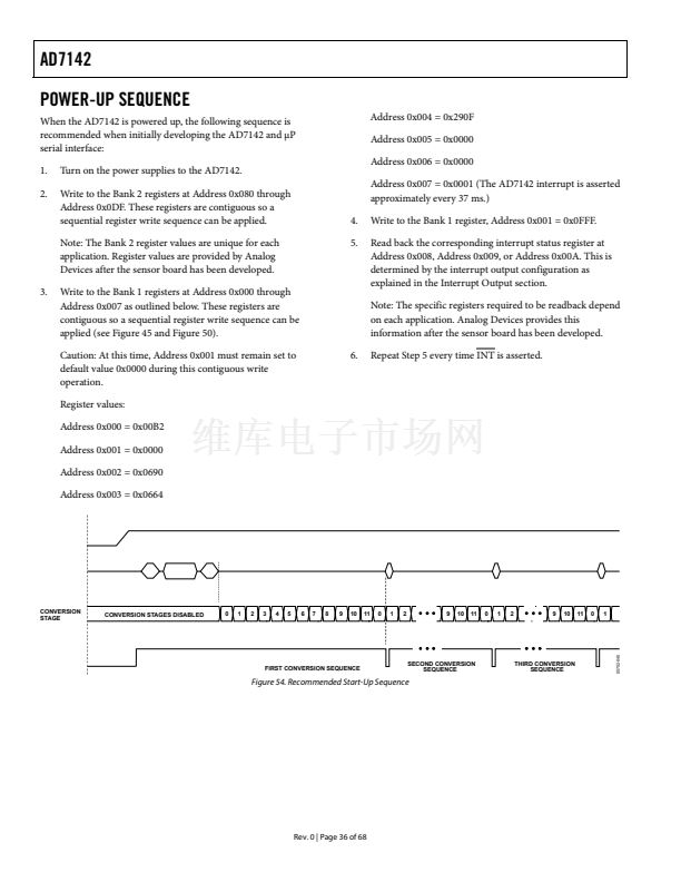
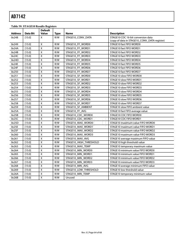
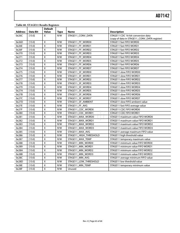
Figure 4. AD7142 Pin Configuration
Figure 5. AD7142-1 Pin Configuration
Table 7. Pin Function Descriptions
Pin No.
REF鈭?/div>
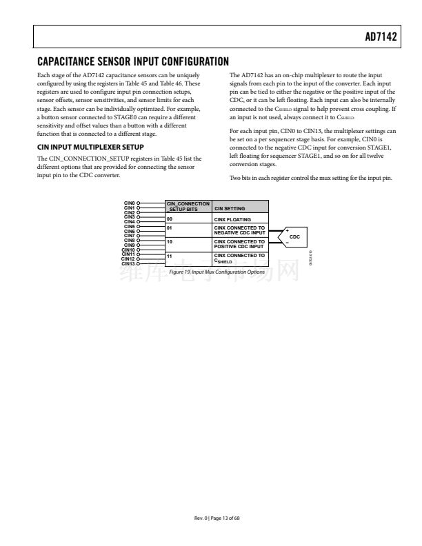
CIN0
CIN1
CIN2
Description
Capacitance Sensor Input.
Capacitance Sensor Input.
Capacitance Sensor Input.
Capacitance Sensor Input.
Capacitance Sensor Input.
Capacitance Sensor Input.
Capacitance Sensor Input.
Capacitance Sensor Input.
Capacitance Sensor Input.
Capacitance Sensor Input.
Capacitance Sensor Input.
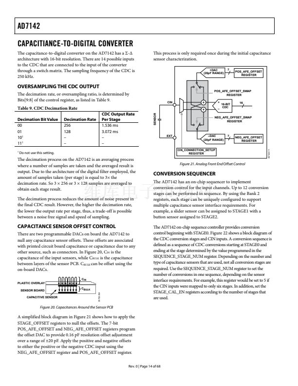
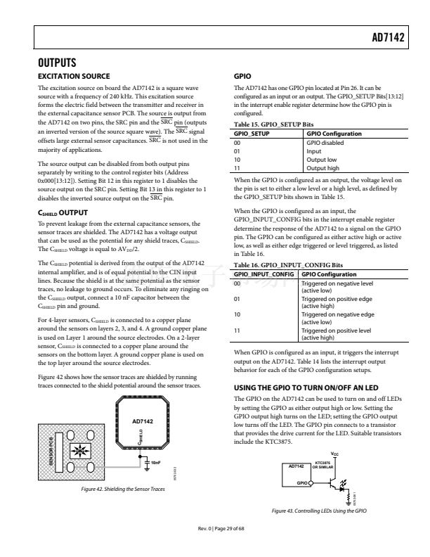
CDC Shield Potential Output. Requires 10 nF capacitor to ground. Connect to external shield.
CDC Supply Voltage.
Analog Ground Reference Point for All CDC Circuitry. Tie to analog ground plane.
CDC Excitation Source Output.
Inverted Excitation Source Output.
Digital Core Supply Voltage.
Digital Ground.
Digital Ground.
Serial Interface Operating Voltage Supply.
AD7142 SPI Serial Data Output.
AD7142-1 I
2
C Serial Data Input/Output. SDA requires pull-up resistor.
AD7142 SPI Serial Data Input.
AD7142-1 I
2
C Address Bit 0.
Clock Input for Serial Interface.
AD7142 SPI Chip Select Signal.
AD7142-1 I
2
C Address Bit 1.
General-Purpose Open-Drain Interrupt Output. Programmable polarity; requires pull-up resistor.
Programmable GPIO.
Factory Test Pin. Tie to ground.
CDC Positive Reference Input. Normally tied to analog power.
CDC Negative Reference Input. Tie to analog ground.
Capacitance Sensor Input.
Capacitance Sensor Input.
Capacitance Sensor Input.
Rev. 0 | Page 8 of 68
05702-044


 1
1
 2
2
 3
3
 4
4
 5
5
 6
6
 7
7
 8
8
 9
9
 10
10
 11
11
 12
12
 13
13
 14
14
 15
15
 16
16
 17
17
 18
18
 19
19
 20
20
 21
21
 22
22
 23
23
 24
24
 25
25
 26
26
 27
27
 28
28
 29
29
 30
30
 31
31
 32
32
 33
33
 34
34
 35
35
 36
36
 37
37
 38
38
 39
39
 40
40
 41
41
 42
42
 43
43
 44
44
 45
45
 46
46
 47
47
 48
48
 49
49
 50
50
 51
51
 52
52
 53
53
 54
54
 55
55
 56
56
 57
57
 58
58
 59
59
 60
60
 61
61
 62
62
 63
63
 64
64
 65
65
 66
66
 67
67
 68
68
