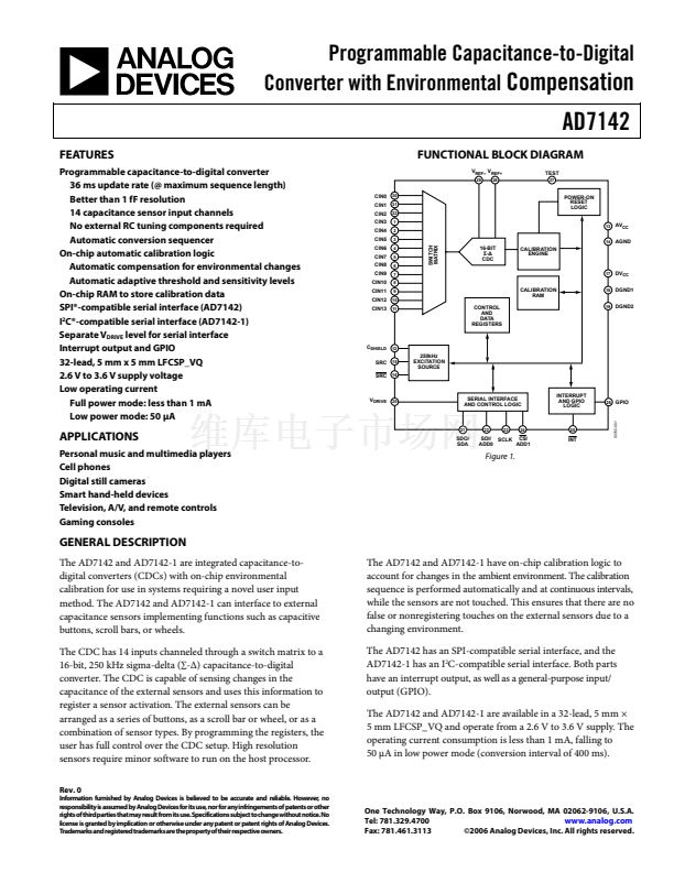
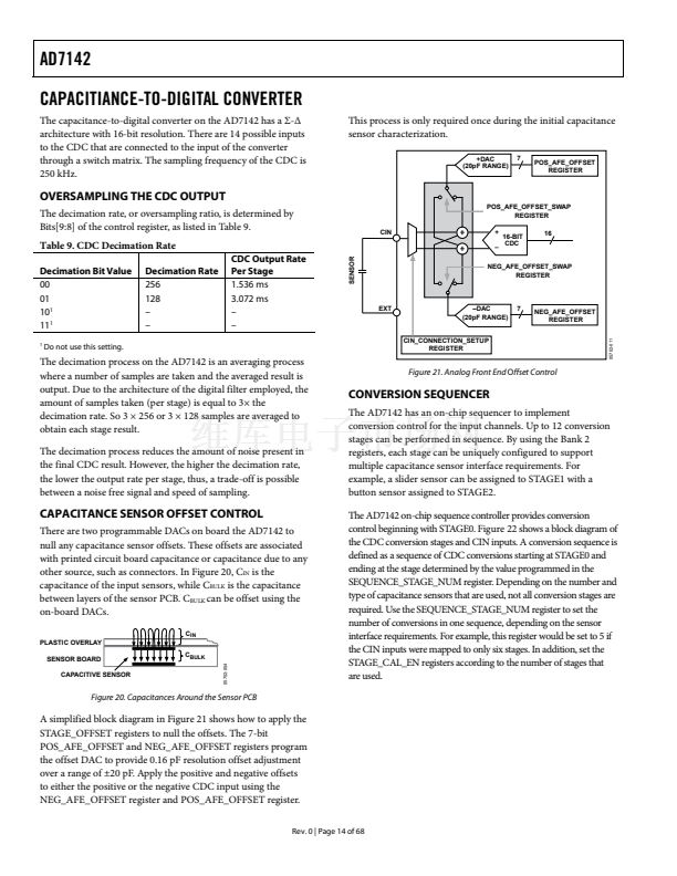
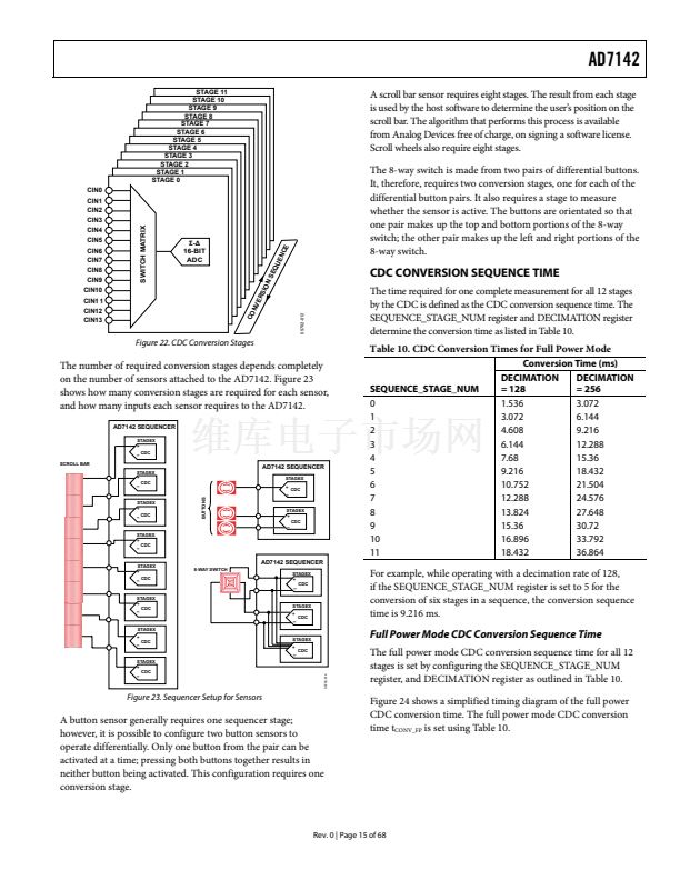
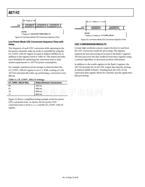
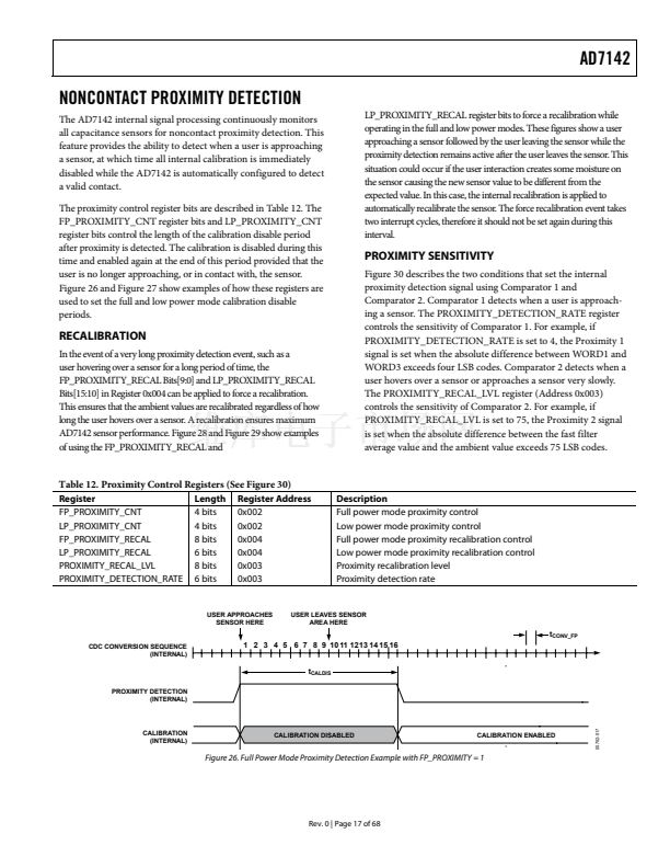
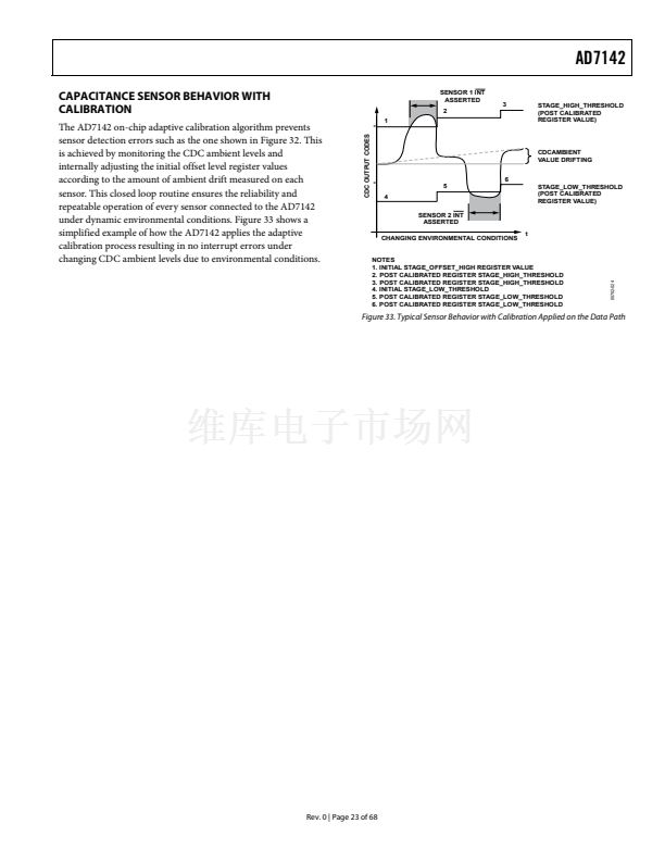
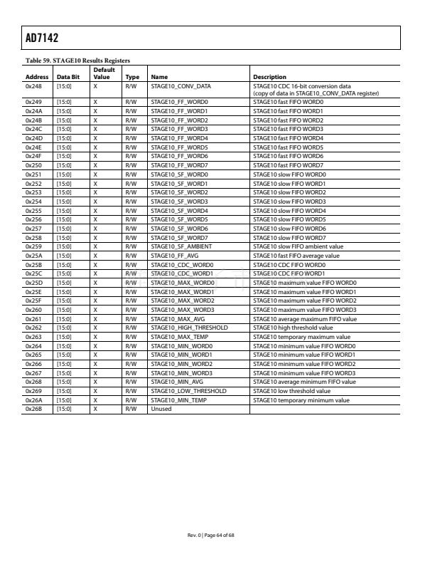
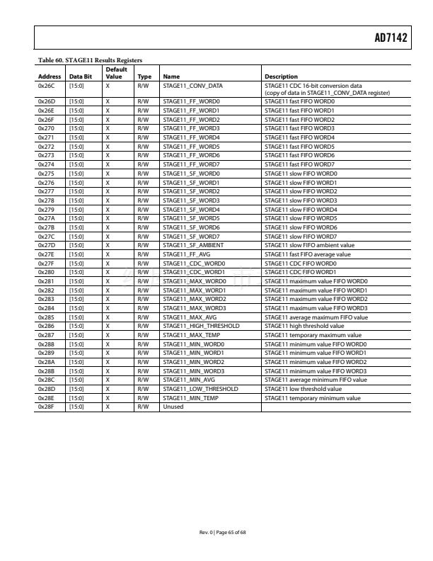
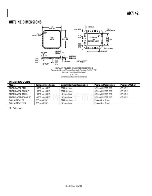
AD7142
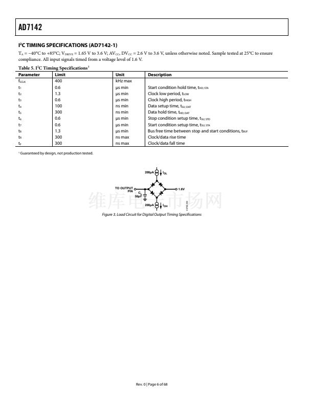
I
2
C TIMING SPECIFICATIONS (AD7142-1)
T
A
= 鈭?0擄C to +85擄C; V
DRIVE
= 1.65 V to 3.6 V; AV
CC
, DV
CC
= 2.6 V to 3.6 V, unless otherwise noted. Sample tested at 25擄C to ensure
compliance. All input signals timed from a voltage level of 1.6 V.
Table 5. I
2
C Timing Specifications
1
Parameter
f
SCLK
t
1
t
2
t
3
t
4
t
5
t
6
t
7
t
8
t
R
t
F
1
Limit
400
0.6
1.3
0.6
100
300
0.6
0.6
1.3
300
300
Unit
kHz max
渭s min
渭s min
渭s min
ns min
ns min
渭s min
渭s min
渭s min
ns max
ns max
Description
Start condition hold time, t
HD; STA
Clock low period, t
LOW
Clock high period, t
HIGH
Data setup time, t
SU; DAT
Data hold time, t
HD; DAT
Stop condition setup time, t
SU; STO
Start condition setup time, t
SU; STA
Bus free time between stop and start conditions, t
BUF
Clock/data rise time
Clock/data fall time
Guaranteed by design, not production tested.
200碌A(chǔ)
I
OL
TO OUTPUT
PIN
1.6V
C
L
50pF
200碌A(chǔ)
I
OH
05702-004
Figure 3. Load Circuit for Digital Output Timing Specifications
Rev. 0 | Page 6 of 68


 1
1
 2
2
 3
3
 4
4
 5
5
 6
6
 7
7
 8
8
 9
9
 10
10
 11
11
 12
12
 13
13
 14
14
 15
15
 16
16
 17
17
 18
18
 19
19
 20
20
 21
21
 22
22
 23
23
 24
24
 25
25
 26
26
 27
27
 28
28
 29
29
 30
30
 31
31
 32
32
 33
33
 34
34
 35
35
 36
36
 37
37
 38
38
 39
39
 40
40
 41
41
 42
42
 43
43
 44
44
 45
45
 46
46
 47
47
 48
48
 49
49
 50
50
 51
51
 52
52
 53
53
 54
54
 55
55
 56
56
 57
57
 58
58
 59
59
 60
60
 61
61
 62
62
 63
63
 64
64
 65
65
 66
66
 67
67
 68
68
